Frequency multiplier for wave-guide structure and manufacturing method thereof
A waveguide structure and frequency multiplier technology, applied in the laser field, can solve the problems of low frequency doubling efficiency and limited effective frequency doubling length, and achieve the effect of improving efficiency
- Summary
- Abstract
- Description
- Claims
- Application Information
AI Technical Summary
Problems solved by technology
Method used
Image
Examples
Embodiment Construction
[0048] The present invention will be further described in conjunction with the accompanying drawings and specific embodiments.
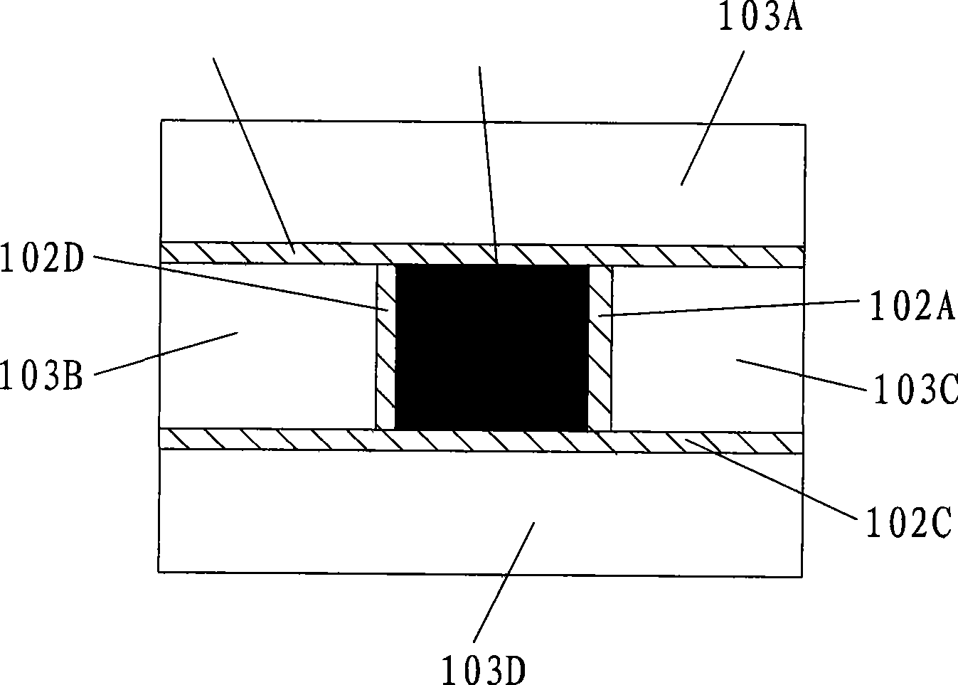
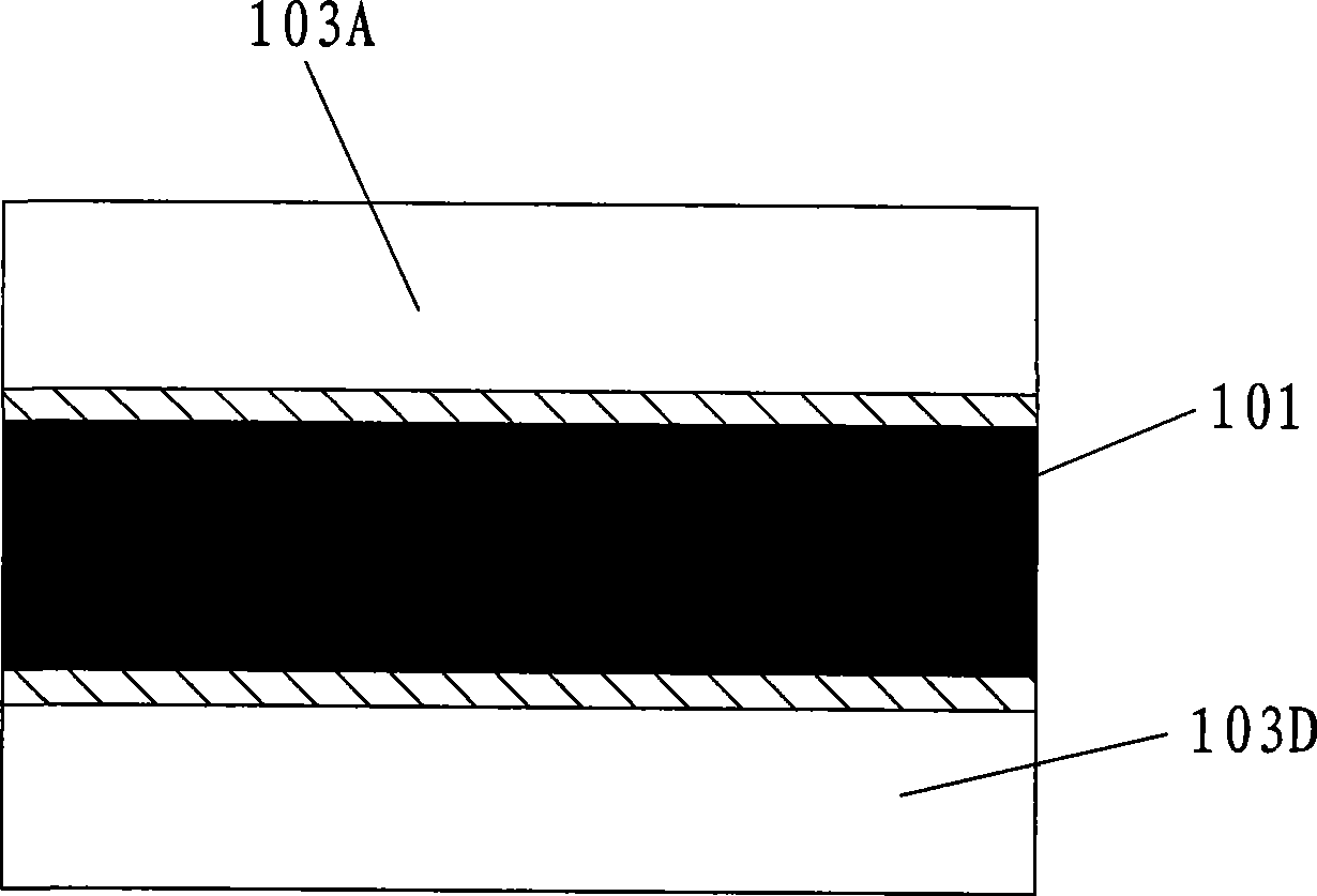
[0049] Referring to Fig. 1(a) and Fig. 1(b), it is a cross-sectional schematic view and a longitudinal sectional view of the frequency multiplier of the present invention. Among them, 101 is the frequency doubling crystal (shown in gray), 102A, 102B, 102C, 102D are glue layers or deepened optical glue layers with a lower refractive index than the frequency doubling crystal 101 (shown in the diagonal line area), 103A, 103B, 103C and 103D are optical materials as substrates.
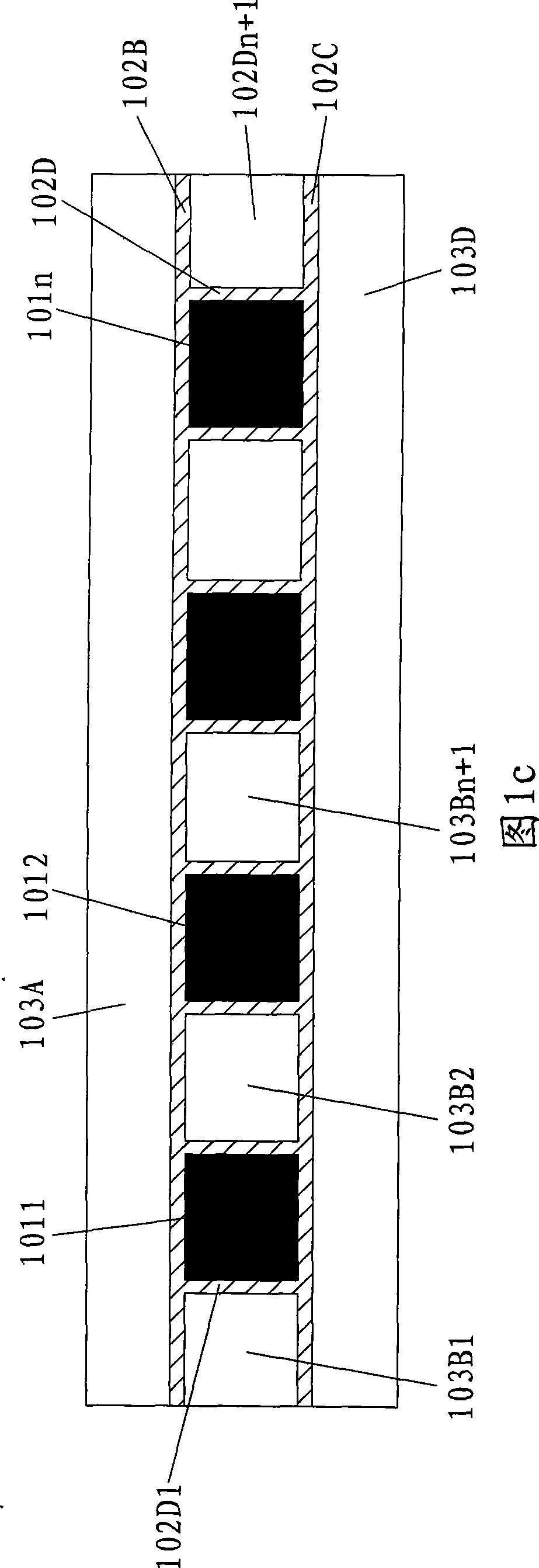
[0050] Referring to Fig. 1(c) and Fig. 1(d), it is a schematic cross-sectional view and a longitudinal sectional view of the array frequency multiplier of the present invention. It is similar in structure to Fig. 1(a) and Fig. 1(b), and it is a frequency doubling crystal waveguide array. Among them, 101 is a frequency doubling crystal, 1011, 1012, ... 101n are a series of frequ...
PUM
 Abstract
Description
Claims
Application Information


