Transparent resistor type non-volatile memory

A non-volatile, memory technology, applied in static memory, digital memory information, information storage, etc., can solve problems such as low read and write speed, low integration, and information loss

Inactive Publication Date: 2009-07-08
INST OF PHYSICS - CHINESE ACAD OF SCI
View PDF0 Cites 18 Cited by
  • Summary
  • Abstract
  • Description
  • Claims
  • Application Information

AI Technical Summary

Problems solved by technology

[0002] A large number of scientific research institutions and companies around the world invest huge manpower and material resources in memory research every year. Among them, DRAM is widely used because of its high integration and high-speed operation, but the stored information will be lost after power off; Compared with DRAM, although flash memory (Flash Memory) has non-volatile characteristics, its integration level is relatively low and its read and write speed is relatively low.

Method used


Image

  • Transparent resistor type non-volatile memory
  • Transparent resistor type non-volatile memory
  • Transparent resistor type non-volatile memory

Examples


Embodiment Construction

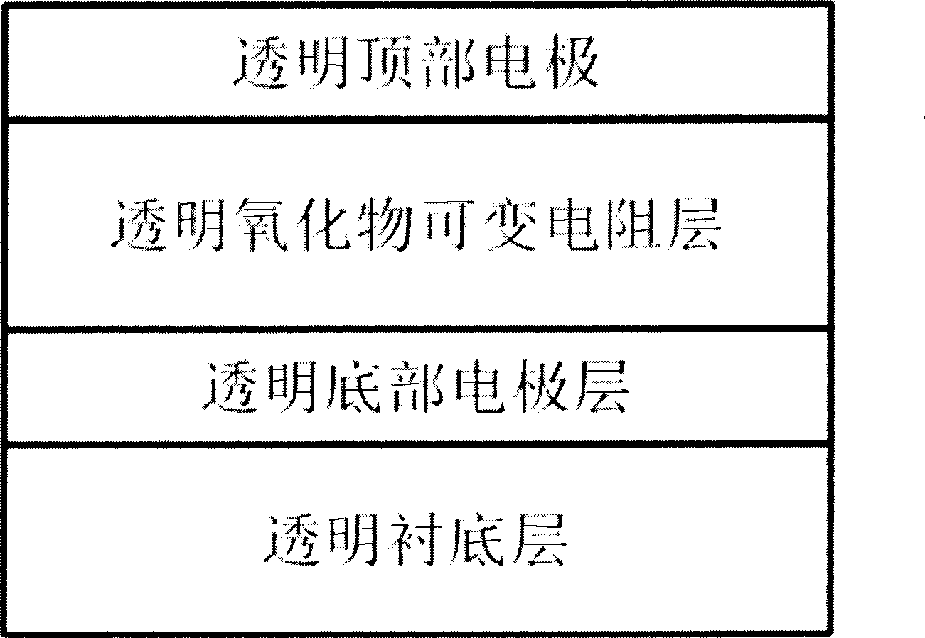
[0024] After the transparent substrate material is cleaned by physical or chemical methods, it is put into a physical or chemical deposition system to form a transparent bottom electrode on the transparent substrate, and a transparent oxide or nitride variable resistance material layer is formed on the transparent bottom electrode. , forming a transparent top electrode on the variable resistance dielectric material layer of transparent oxide or nitride, and forming required devices by photolithography technology.

[0025] For clarity, figure 1 Device width and thickness are exaggerated.

[0026] figure 1 A schematic structural diagram of a transparent resistive nonvolatile memory according to an embodiment of the present invention is shown.

[0027] refer to figure 1 , The transparent resistive nonvolatile memory according to the embodiment of the present invention includes a transparent substrate layer, a transparent bottom electrode layer, a transparent oxide or nitride v...


PUM


Abstract

The invention discloses a completely transparent nonvolatile memory, which comprises a transparent substrate, a transparent bottom electrode layer formed on the substrate, a transparent record medium layer formed on the bottom electrode, and a transparent top electrode layer formed on the transparent record medium layer, wherein, the transparent substrate is an insulator; and the transparent record medium layer has the properties of variable resistors. The transparent memory not only has the characteristics of RRAM (resistance random access memory) but also has good light transmittance. Accordingly, the transparent memory can be widely used in the field of photoelectrical display, photoelectrical storage and other transparent electronic product field to provide effective path for the integration of optical products and memories.

Description

technical field [0001] The invention relates to a nonvolatile memory, more specifically to a transparent resistance nonvolatile memory. Background technique [0002] A large number of scientific research institutions and companies around the world invest huge manpower and material resources in memory research every year. Among them, DRAM is widely used because of its high integration and high-speed operation, but the stored information will be lost after power off; Compared with DRAM, although flash memory (Flash Memory) has the characteristics of non-volatility, its integration level is relatively low and its reading and writing speed is relatively low. Currently, among various nonvolatile memories being studied, resistive random access memory (RRAM) is considered to be the most potential next-generation nonvolatile memory because of its multiple advantages. Compared with other non-volatile random access memories, from the perspective of technical performance, RRAM not onl...

Claims


Application Information

Patent Timeline
Patent Type & Authority Applications(China)
IPC IPC(8): H01L45/00H01L27/24G11C11/56
Inventor 孟洋赵宏武张培健刘紫玉廖昭亮潘新宇梁学锦陈东敏
Owner INST OF PHYSICS - CHINESE ACAD OF SCI
Why Eureka
Try Eureka