Multilayer printed wiring board, solder resist composition, method for manufacturing multilayer printed wiring board, and semiconductor device
A multi-layer printing and circuit board technology, which is applied in the direction of multi-layer circuit manufacturing, printed circuit secondary treatment, non-metallic protective layer coating, etc., can solve the problem that multi-layer printed circuit boards are difficult to meet the flame retardancy and other problems
- Summary
- Abstract
- Description
- Claims
- Application Information
AI Technical Summary
Problems solved by technology
Method used
Image

Examples
example 1
[0378] A. Preparation of resin formulation for upper roughened surface structure
[0379] (i) 25% acrylated cresol novolac acrylate novolac epoxy resin (produced by Nippon Kayaku, molecular weight 2,500) dissolved in diglyme (DMDG) with 35 parts by weight of 80 wt% concentration ) produced resin solution, 3.15 parts by weight of photosensitive monomer (produced by Toagosei Chemical Company, Aronix M315), 0.5 parts by weight of defoamer (produced by SanNopco Company, S-65), and 3.6 parts by weight of N Methylpyrrolidone (NMP) was placed in a container to mix and stir to make a blended formulation.
[0380] (ii) 12 parts by weight of polysulfone (PSF), 7.2 parts by weight of epoxy resin particles (produced by Sanyo Chemical Co., Polymerpol) with an average particle size of 0.1 μm, and 3.09 parts by weight of epoxy resin particles with an average particle size of 0.5 μm Epoxy resin particles were put into another container and mixed and stirred into a mixture, then 30 parts by w...
example 2
[0437] A. The preparation of the resin formulation for the roughened surface structure of the upper and lower layers and the preparation of the resin filler were carried out in the same manner as discussed in Example 1.
[0438] B. Methods for Manufacturing Multilayer Printed Circuit Boards
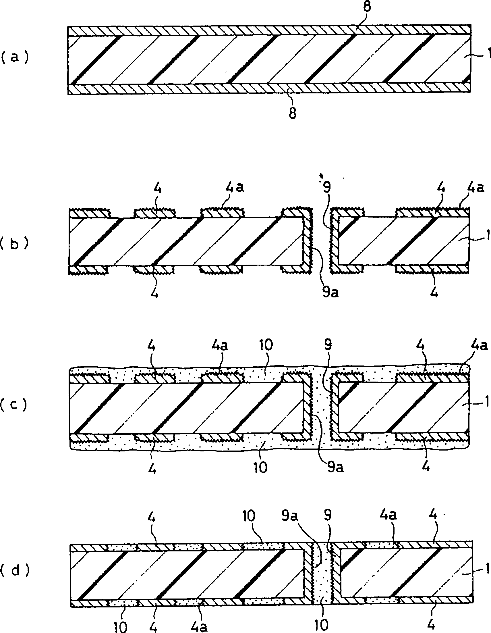
[0439] (1) A copper-laminated laminate is used as a raw material, which consists of a substrate 1 made of 1mm-thick glass epoxy resin or BT (bismaleimide triazine) resin and layers on both sides of the substrate 1 Composed of copper foil 8 with a thickness of 18 μm (refer to Image 6 (a)). Firstly, holes are drilled on the copper laminate to form through holes, and electroless plating is performed, followed by pattern etching to form the lower layer conductive circuit 14 and plated through holes 9 on both sides of the substrate 1 .
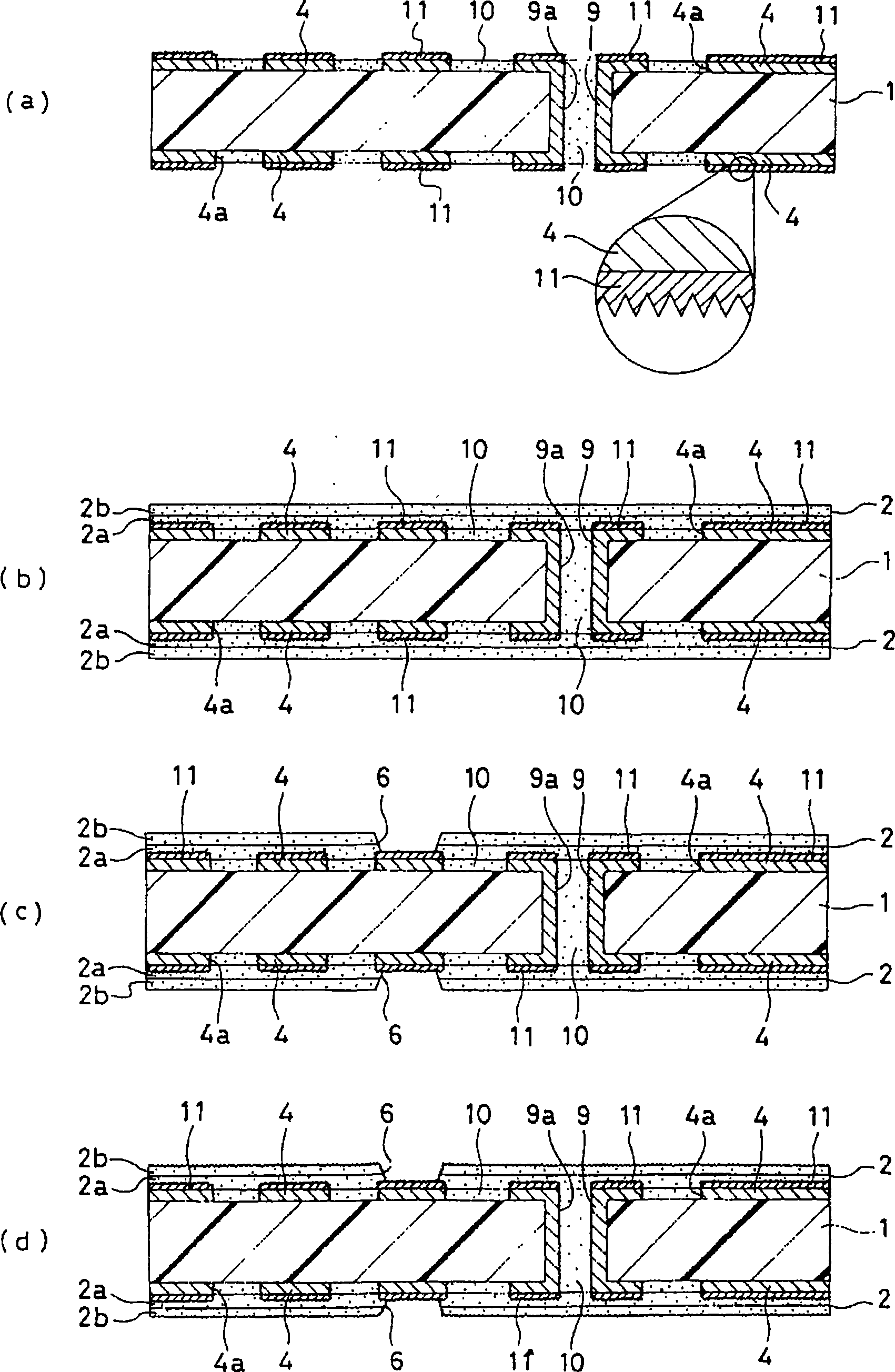
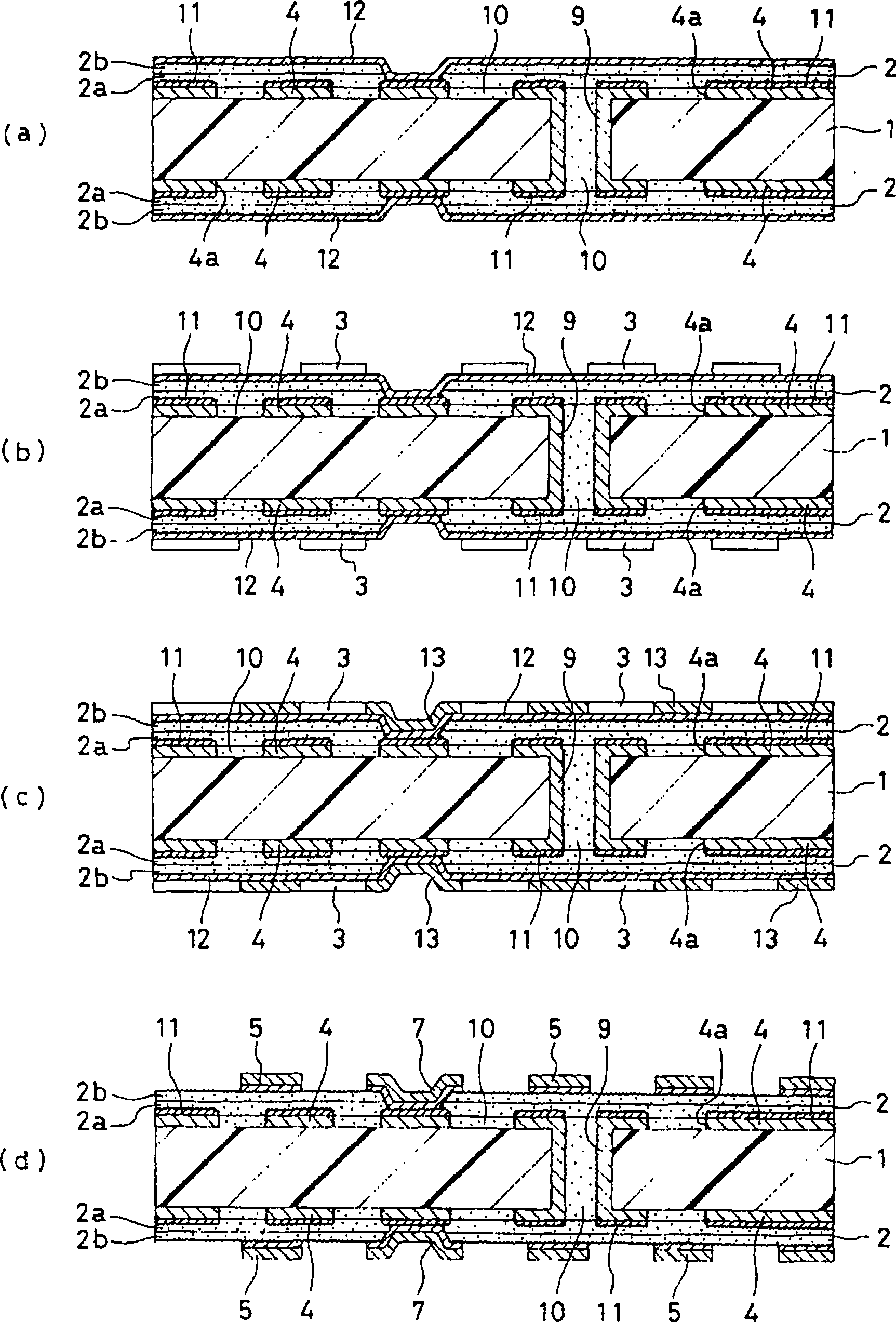
[0440] (2) Clean and dry the synthetic substrate that has been made into the plated through hole 9 and the lower layer conductive circuit 14 with water, th...
example 3
[0482] Adopt the same method of Example 1 to manufacture a multilayer printed circuit board, except adding 7 parts by weight of epoxy-terminated polybutadiene as an elastomer in the process of solder mask formulation preparation in step (16).
PUM
 Abstract
Description
Claims
Application Information
PatSnap Eureka turns technology decisions into work you can execute. Powered by our Innovation Knowledge Graph, it runs expert workflows across engineering, life sciences, materials and intellectual property. Get your review-ready output in minutes.


