Time clock generating circuit and design method

A technology of clock generation circuit and design method, applied to electrical components, single output arrangement, devices that give pulses at different times, etc., can solve the problems of increasing chip manufacturing cost, large chip area, increasing circuit power consumption, etc., to achieve The effect of improving performance, reducing production cost, and reducing chip area

Inactive Publication Date: 2009-07-22
修思(北京)电影科技有限公司
View PDF0 Cites 5 Cited by
  • Summary
  • Abstract
  • Description
  • Claims
  • Application Information

AI Technical Summary

Problems solved by technology

However, these too many inverters composed of large-size CMOS transistors will occupy a large chip area, increase the manufacturing cost of the chip, and also increase the power consumption of the circuit, which is not conducive to the design and application of low-power chips.

Method used


Image

  • Time clock generating circuit and design method
  • Time clock generating circuit and design method
  • Time clock generating circuit and design method

Examples


Embodiment Construction

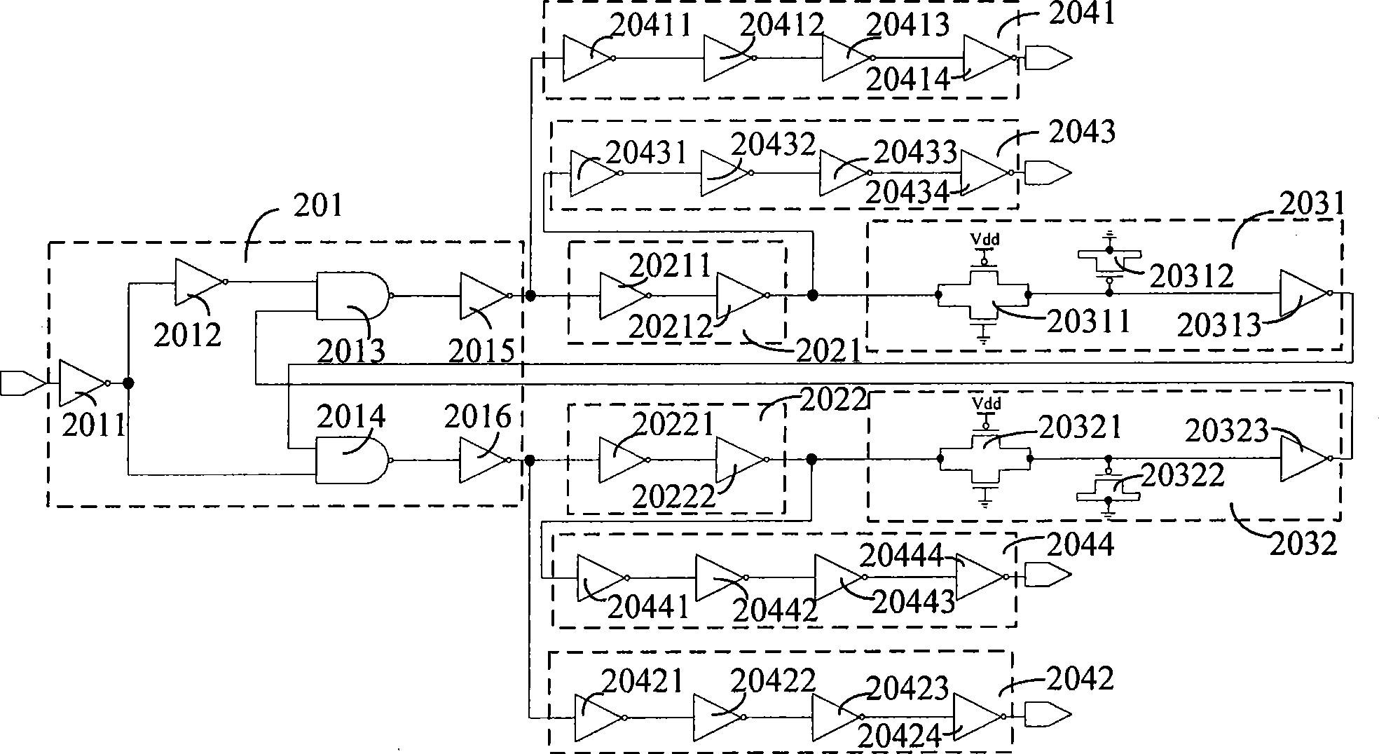
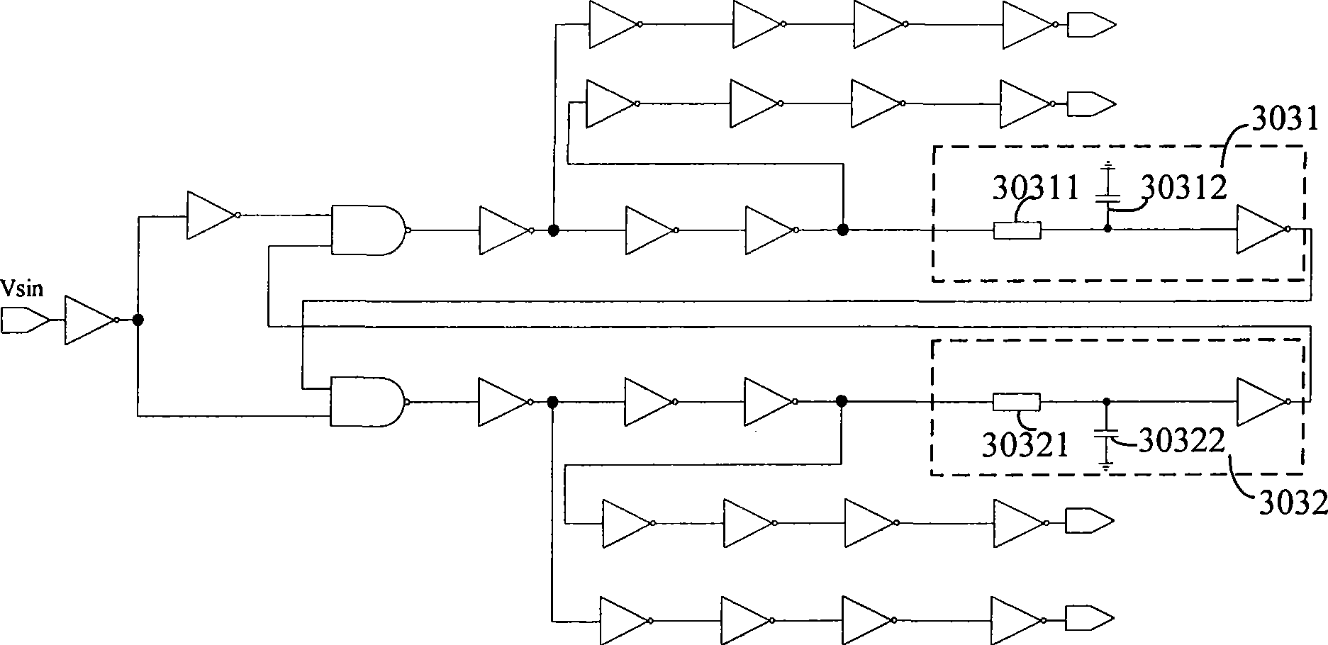
[0037] The present invention is based on the existing clock generating circuit, through a transmission gate composed of a CMOS transistor connected in series and a PMOS transistor instead of a plurality of large-sized CMOS transistor inverters in the delay module of the clock circuit to form a low-pass RC The circuit realizes the delay function in the process of generating the clock signal.

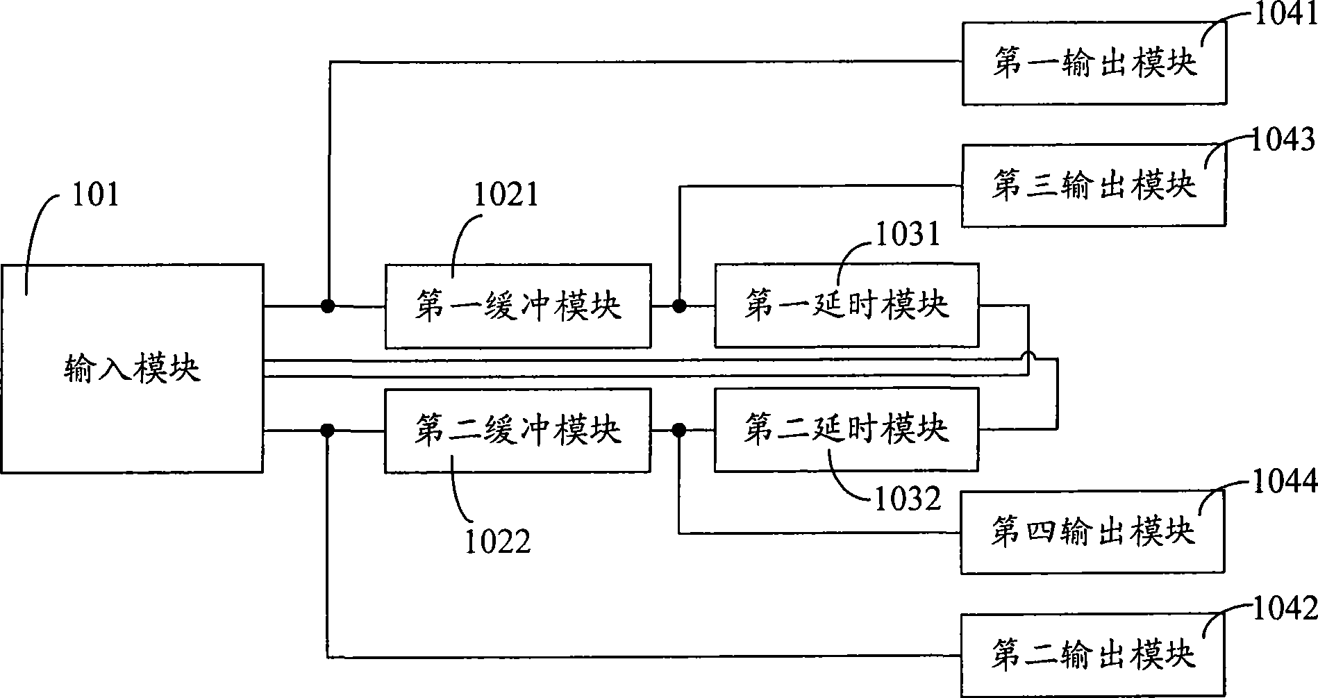
[0038] figure 1 It is a structural block diagram of a clock generation circuit in a specific embodiment of the present invention, the clock generation circuit includes an input module 101, a first buffer module 1021, a second buffer module 1022, a first delay module 1031, a second delay module 1032 and a first An output module 1041 , a second output module 1042 , a third output module 1043 , and a fourth output module 1044 . in,

[0039] An input module 101, configured to generate a first clock signal and a second clock signal;

[0040] The first buffer module 1021 is configured to gen...


PUM


Abstract

The invention discloses a clock generating circuit and a design method thereof which comprises the following steps that an input module comprising a dispersion gate and an inverter is built, and a clock signal, which is received by the input module is transmitted into a buffer module and an output module according to an input signal; the buffer module comprising a plurality of inverters is built, and a buffer signal which is received by the buffer module, is generated according to the clock signal; the output module comprising a plurality of inverters is built, and clock signals, which are not mutually overlapped and are received by the output module, are buffered and output according to the clock signal and the buffer signal; a delay module comprising a transfer gate and a PMOS transistor is built, and a delay signal is generated by delaying the clock signal by the delay module, wherein, the output module, the buffer module and the delay module are connected in sequence, and the delay signal generated from the delay module is fed back to the input module as an input signal. Through adopting the clock generating circuit and the design method thereof, the performance of the clock generating circuit is improved and the chip space and the production cost of the chip are reduced.

Description

technical field [0001] The invention mainly relates to the field of integrated circuits, in particular to a clock generation circuit and a design method. Background technique [0002] In ∑-△ analog-to-digital converter (ADC, Analog-to-Digital Converter) circuits, a switched capacitor integrator circuit is commonly used. In order to realize this integrator, a clock generation circuit is an essential circuit module. In order for the switched capacitor integrator circuit to work normally and achieve high performance, it is necessary to generate a clock signal with two non-overlapping phases, that is, two such clock signals are mutually inverse signals, and the two clock signals will not be high at the same time. If the clock signal is not well designed and the two clock signals overlap each other, it will cause leakage in the integration process, thereby introducing unnecessary noise into the signal and affecting the performance of the switched capacitor integrator circuit. ...

Claims


Application Information

Patent Timeline
Patent Type & Authority Applications(China)
IPC IPC(8): H03K5/151H03K5/13H03M3/02H03K5/135H03K5/14
Inventor 罗晋张信盛世敏张现聚
Owner 修思(北京)电影科技有限公司
Why Eureka
Try Eureka