
Manufacturing method of circuit board without tin plating and tin removing

A circuit board and tin stripping technology, which is applied to the removal of conductive materials by chemical/electrolytic methods, can solve problems such as increased production costs, waste of precious metal chemical materials, environmental pollution, etc., to reduce pollution, achieve clean production, and avoid serious problems. The effect of pollution

Inactive Publication Date: 2011-04-06
陈国富
View PDF0 Cites 0 Cited by
  • Summary
  • Abstract
  • Description
  • Claims
  • Application Information

AI Technical Summary

Problems solved by technology

It can be seen that the traditional process not only causes serious environmental pollution, but also causes a lot of waste of precious metals, water, electricity, and chemical materials, which greatly increases the production cost of enterprises.

Method used

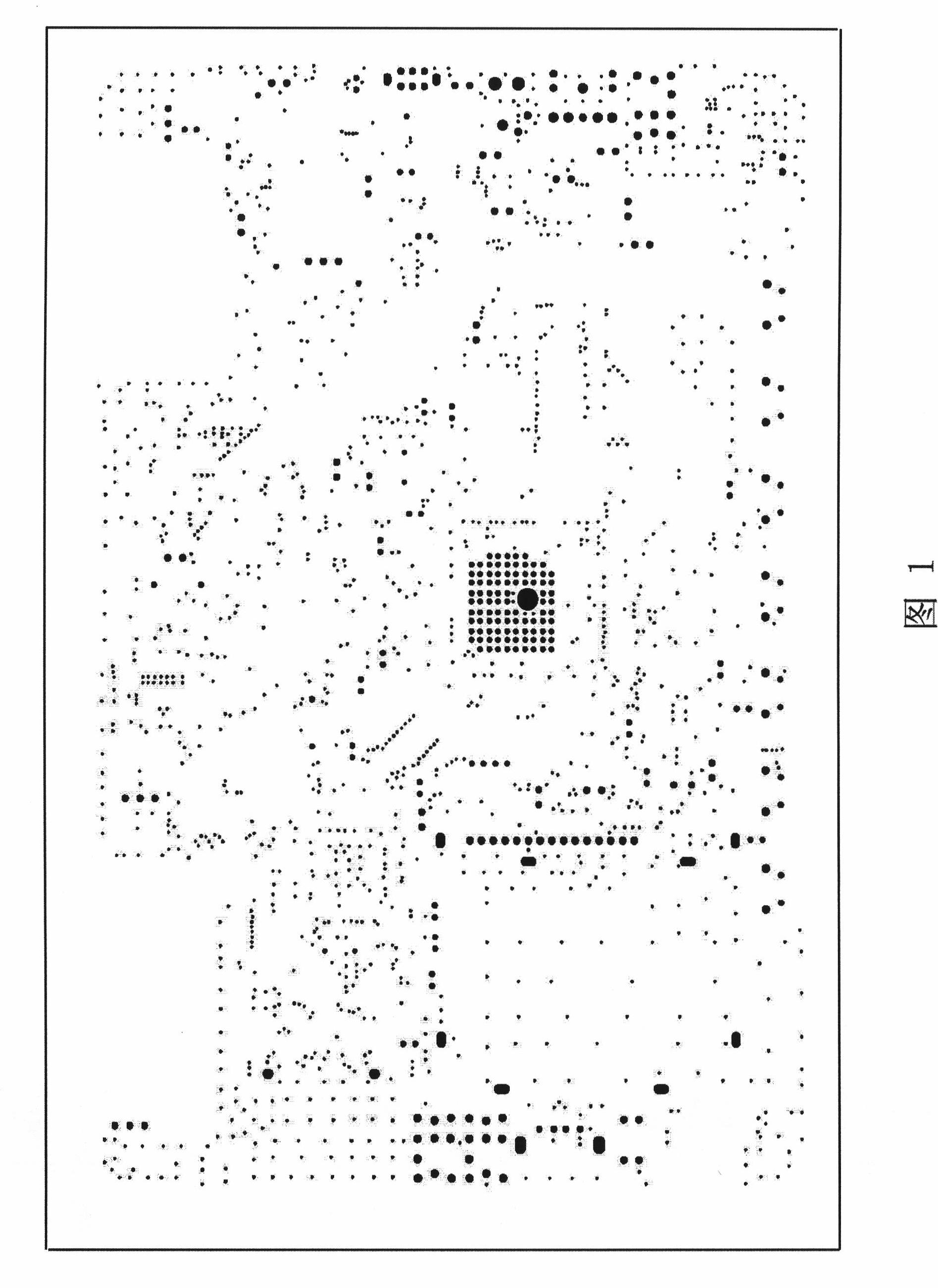
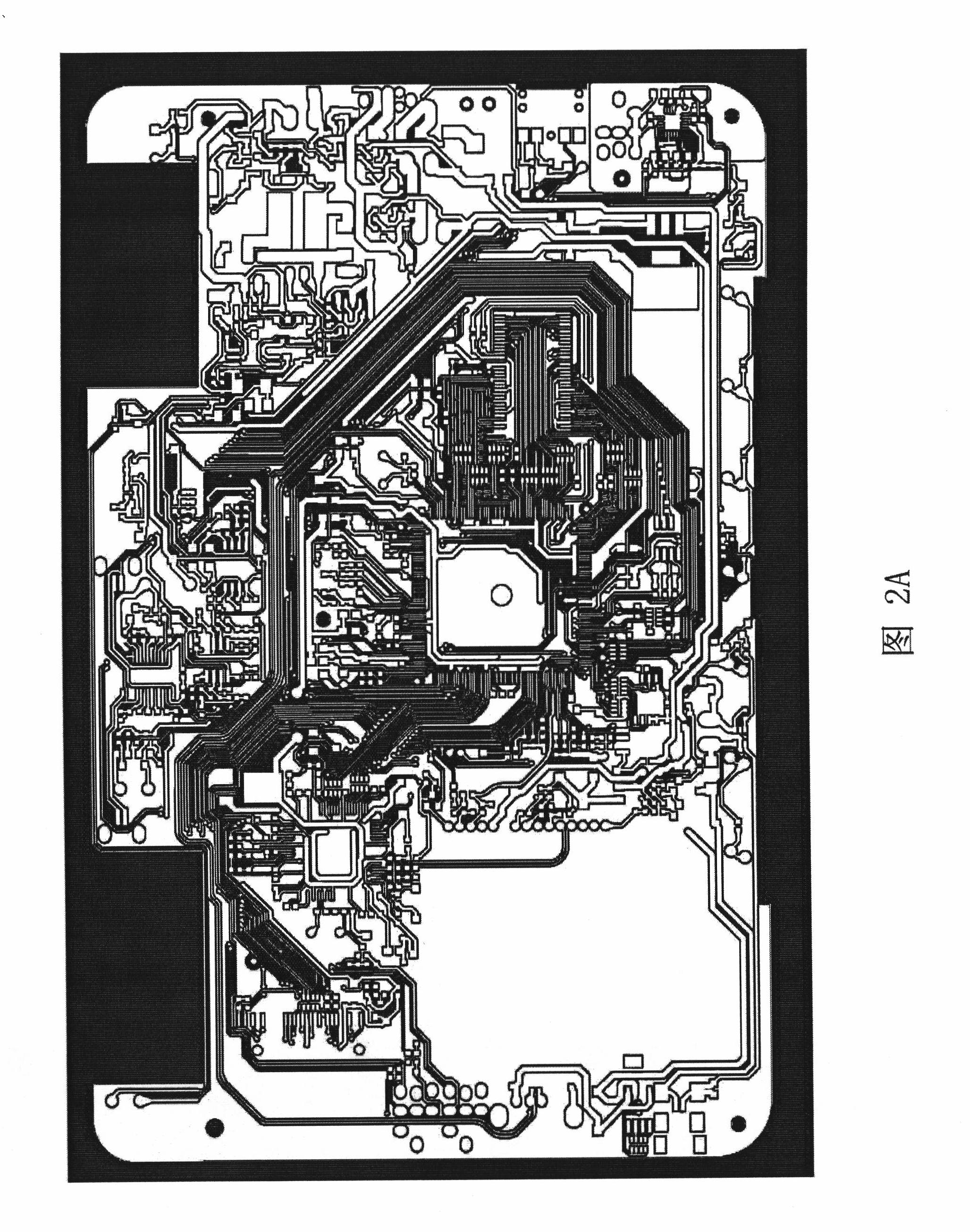
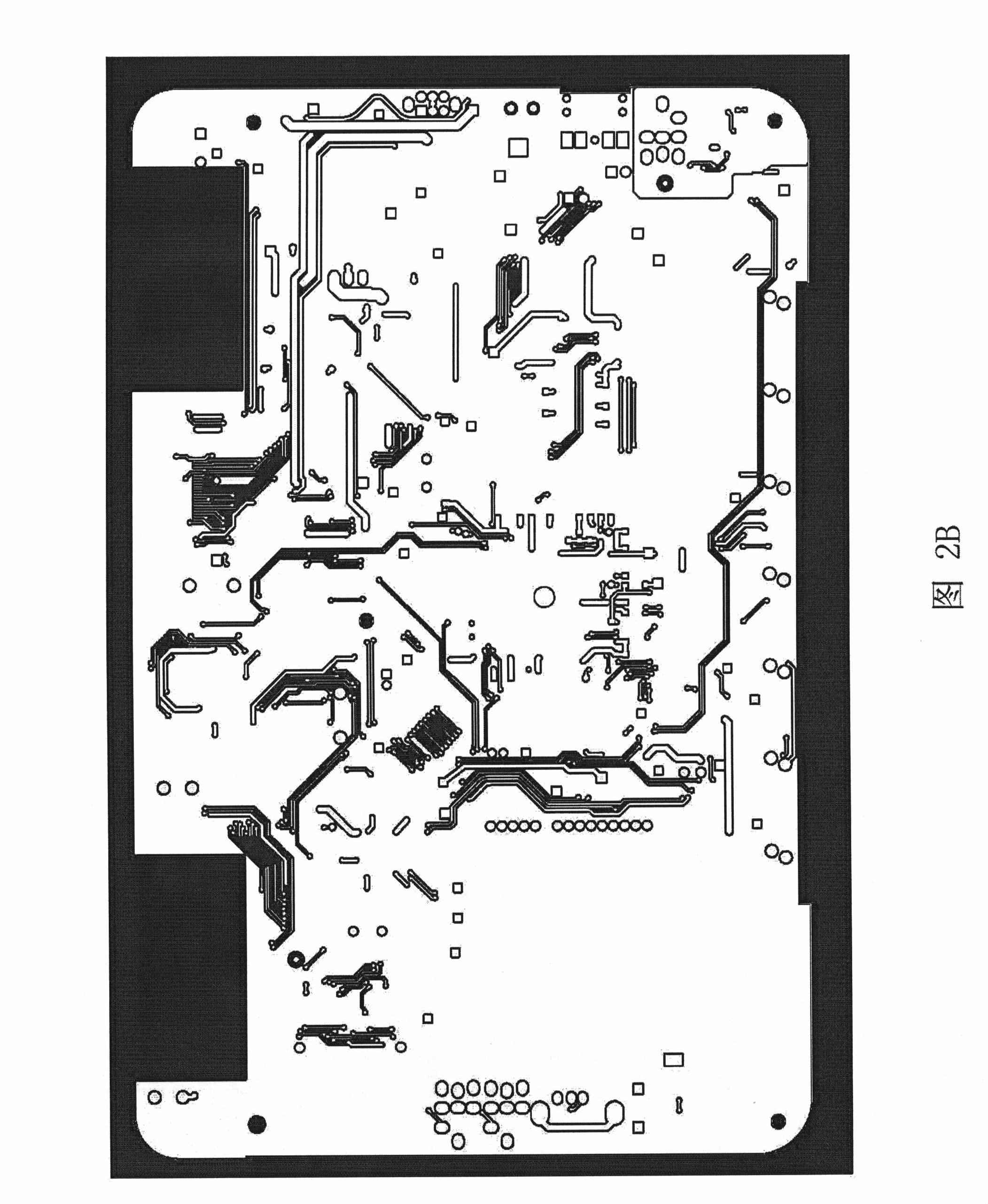

Image

  • Manufacturing method of circuit board without tin plating and tin removing
  • Manufacturing method of circuit board without tin plating and tin removing
  • Manufacturing method of circuit board without tin plating and tin removing

Examples


Embodiment Construction

[0016] The following examples are further explanations and illustrations of the present invention, and do not constitute any limitation to the present invention.

[0017] The manufacturing method of the circuit board exempt from tin plating and stripping of the present invention (taking double-sided panels as an example), the steps are as follows:

[0018] First, drill holes on the cut and baked copper clad board according to the program compiled by the user, and then carry out thick copper treatment on the drilled holes to make the circuits on both sides of the copper clad board conduct. This step is similar to the conventional method.

[0019] The gist of the present invention is to remove the electroplating tin and tin stripping process in the traditional circuit board manufacturing process, and selectively electroplate copper and nickel to the circuit pattern. The specific steps are:

[0020] 1. Coating a layer of anti-plating covering film on the circuit board that has be...


PUM


Abstract

A method for manufacturing circuit board which is free of tin plating and tin removing comprises the following steps: a. coating plating-resistant covering film on the circuit board after copper deposition or the first time of copper plating, then adhibiting the positive film of all metal holes and hole rings in the circuit pattern on the covering film for forming a primary circuit after exposing and developing; b. electroplating copper and nickel on the hole wall and hole ring of all metal holes, then removing the covering film; c. coating etching-resistant covering film on the circuit board after film removing, adhibiting the negative film of circuit pattern on the etching-resistant covering film, and forming the secondary circuit after exposing and developing; d. etching the circuit pattern, then removing film and checking erosion; and e. forming the finished product of circuit board through executing the steps of resistance welding, exposing, developing, printing component symbol or tin spraying or executing oxidation prevention procession. The method of the invention can reduce environment pollution and realize clean production through eliminating electrotinning and tin removing technique, effectively saves metal, water, electricity and chemical material and reduces production cost of enterprise through selectively electroplating copper and nickel.

Description

【Technical field】 [0001] The present invention relates to a printed circuit board (PCB), in particular to a process that eliminates tin plating and stripping tin, and greatly reduces the area of ​​copper and nickel to be plated by about 90%, thus effectively saving tin, nickel, copper and other precious metals The amount of circuit board production method. 【Background technique】 [0002] As we all know, printed circuit boards (PCBs) are widely used as the basic material of the electronics industry. As small as electronic watches, calculators, personal computers, as large as computers, communication equipment, medical equipment, and aerospace or military equipment, as long as there are electronic components such as integrated circuits, PCBs are used for electrical interconnection between them. Printed circuit boards are formed by setting conductive patterns for electrical connections between electronic components on an insulating substrate, and its manufacturing process is r...

Claims


Application Information

Patent Timeline
Patent Type & Authority Patents(China)
IPC IPC(8): H05K3/06
Inventor 陈国富
Owner 陈国富
Learn More