

Oscillator circuit having frequency jitter characteristic
A frequency jittering and oscillator technology, applied in output power conversion devices, converting continuous pulse trains into pulse train devices with required modes, electrical components, etc., can solve the problems of increasing chip area, high cost, and saving The effect of chip area and simple structure
- Summary
- Abstract
- Description
- Claims
- Application Information
AI Technical Summary
Problems solved by technology
Method used
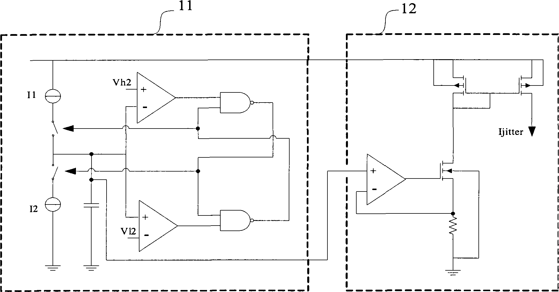
Image

Examples
Embodiment Construction
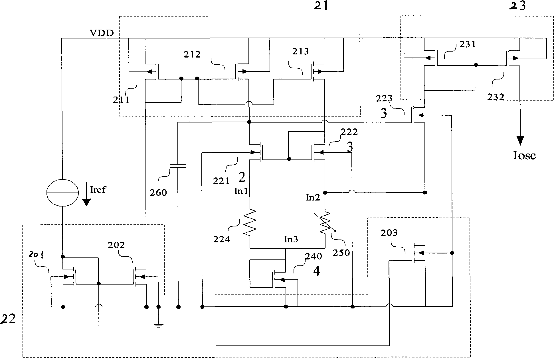
[0022] figure 2 It is a specific realization diagram of the reference current modulation circuit in the present invention. Wherein PMOS transistor 211, PMOS transistor 212 and PMOS transistor 213 form the first group of current mirror 21, NMOS transistor 201, NMOS transistor 202 and NMOS transistor 203 form the second group of current mirror 22, PMOS transistor 231 and PMOS transistor 232 form the third group current mirror 23. The input end of the second set of current mirrors 22 is connected to a reference current Iref. The output end of the third group of current mirrors 23 is the current Iosc, which is output to the oscillator main circuit ( Figure 750) of the current. The NMOS transistor 221 , the NMOS transistor 222 , the NMOS transistor 223 , the resistor 224 , the compensation capacitor 260 and the variable resistor network 250 form a negative feedback control loop. Wherein, the NMOS transistor 240 is to ensure that the NMOS transistor 203 works in a saturation r...
PUM
 Abstract
Description
Claims
Application Information