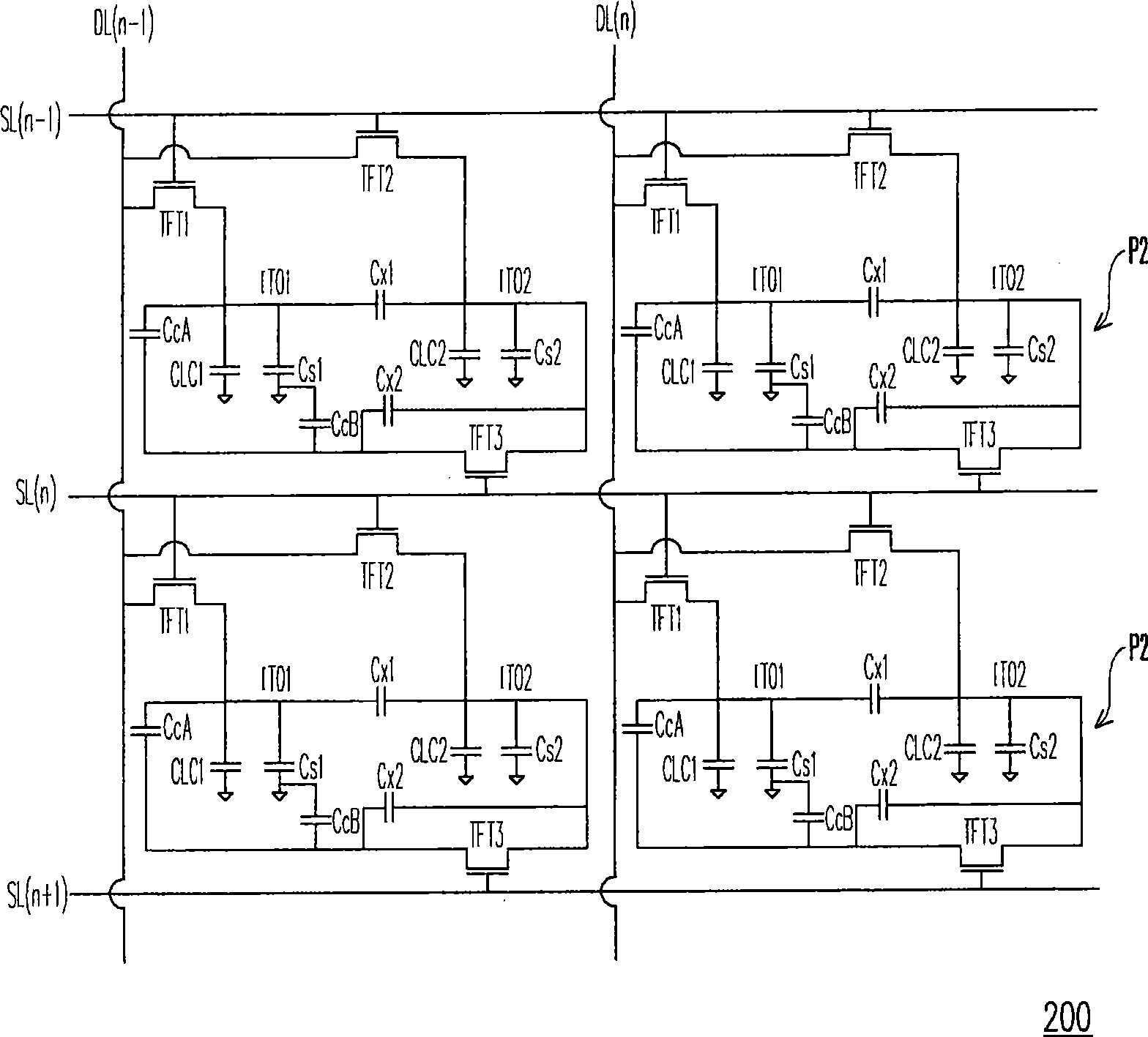
Pixel array, LCD panel and optoelectronic device
A pixel array and pixel electrical technology, which is applied in the field of pixel array, can solve the problem that the color shift problem cannot be effectively improved, and the voltage difference is reduced.
- Summary
- Abstract
- Description
- Claims
- Application Information
AI Technical Summary
Problems solved by technology
Method used
Image

Examples
no. 1 example
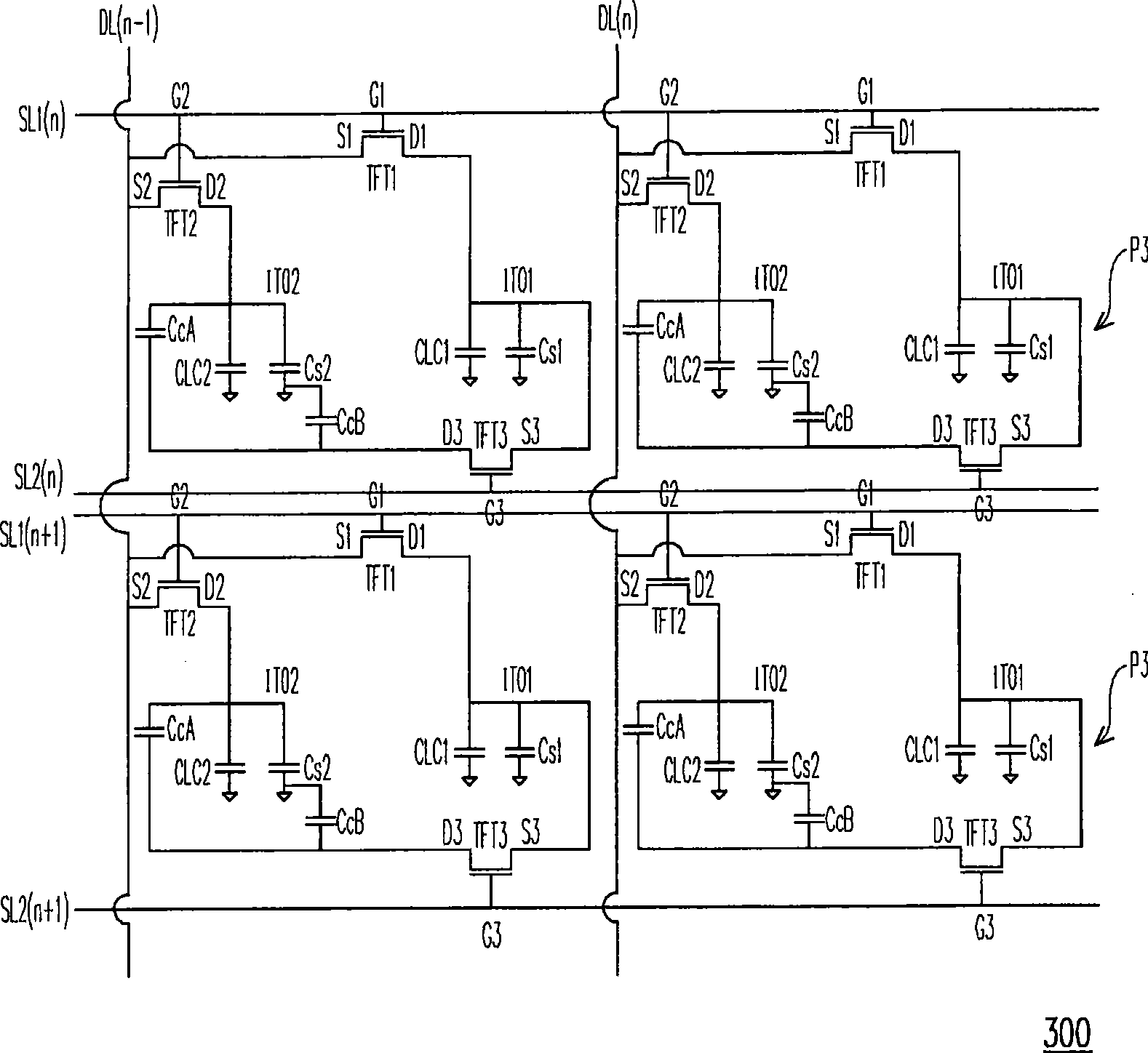
[0069] Figure 3A is an equivalent circuit diagram of the pixel array in the first embodiment of the present invention, Figure 3B is a schematic diagram of the pixel array of the first embodiment of the present invention, and Figure 3B' for along Figure 3B The cross-sectional schematic diagram of the A-A' section line in the middle. Please also refer to Figure 3A and Figure 3B , the pixel array 300 of this embodiment includes a plurality of first scan lines SL1 , a plurality of second scan lines SL2 , a plurality of data lines DL and a plurality of sub-pixels P3 . Here, the first scan line SL1 includes first scan lines SL1(1)˜SL1(n+1), the second scan line SL2 includes second scan lines SL2(1)˜SL2(n), and the data line DL includes Data lines DL(1)˜DL(n). Figure 3A and Figure 3B Only part of the first scan line SL1 , the second scan line SL2 and the data line DL are shown in FIG.
[0070] Each second scan line SL2 is respectively located between two adjacent firs...
no. 2 example
[0084] Figure 5A is an equivalent circuit diagram of the pixel array of the second embodiment of the present invention, Figure 5B is a schematic diagram of a pixel array according to a second embodiment of the present invention, Figure 5B' for along Figure 5B The cross-sectional schematic diagram of the B-B' section line in the middle, and Figure 5C and Figure 5D for Figure 5B Schematic diagram of a single subpixel in . Please refer to Figure 5A to Figure 5C , the pixel array 500 of this embodiment is similar to the pixel array 300 of the first embodiment, but the main difference between the two is that: the second pixel electrode ITO2 in each sub-pixel P4 is located between the first scanning line SL1 and the second scanning line Between SL2. Specifically, the third source S3 of the third thin film transistor TFT3 is directly electrically connected to the first drain D1 across the second pixel electrode ITO2 (such as Figure 5C As shown), at this time, a paras...
no. 3 example
[0088] Figure 7 It is a schematic diagram of the polymer stabilized alignment liquid crystal display panel of the present invention. Please refer to Figure 7 The polymer stabilized alignment liquid crystal display panel 600 of this embodiment includes a first substrate 610 , a second substrate 620 , two polymer stabilized alignment layers 630 , 640 and a liquid crystal layer 650 . The first substrate 610 has the pixel array (300 or 400) in the aforementioned first embodiment or the second embodiment, the second substrate 620 is disposed above the first substrate 610, and two polymer stable alignment layers 630, 640 are respectively disposed on On the first substrate 610 and the second substrate 620 . In addition, the liquid crystal layer 650 is disposed between the two polymer stable alignment layers 630 and 640 . It is worth noting that the liquid crystal layer 650 is manufactured using a liquid crystal material that contains monomers that can be polymerized by an energy...
PUM
 Abstract
Description
Claims
Application Information
 - R&D Engineer
- R&D Manager
- IP Professional
- Industry Leading Data Capabilities
- Powerful AI technology
- Patent DNA Extraction
Browse by: Latest US Patents, China's latest patents, Technical Efficacy Thesaurus, Application Domain, Technology Topic.
© 2024 PatSnap. All rights reserved.Legal|Privacy policy|Modern Slavery Act Transparency Statement|Sitemap