Optical film cutting method and optical film

A cutting method and optical film technology, applied in the field of optical film, can solve the problems of lower productivity of liquid crystal panels, display defects of liquid crystal panels, etc.

Active Publication Date: 2009-08-12
NITTO DENKO CORP
View PDF2 Cites 14 Cited by
  • Summary
  • Abstract
  • Description
  • Claims
  • Application Information

AI Technical Summary

Problems solved by technology

When shavings enter the interior of the liquid crystal panel, display defects of the liquid crystal panel occur, resulting in a problem that the productivity of the liquid crystal panel decreases

Method used


Image

  • Optical film cutting method and optical film

Examples


Embodiment 1

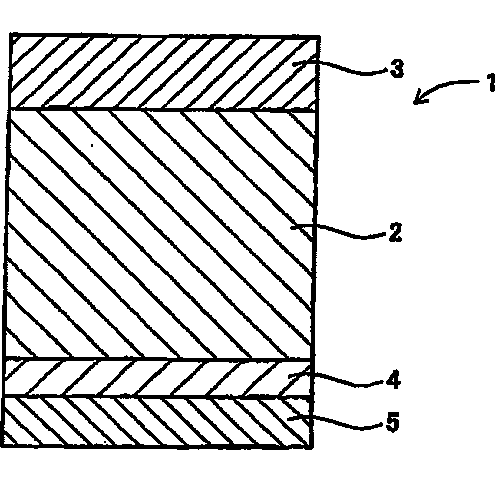
[0051] (production of polarizing plates)

[0052] A polarizer was produced by stretching a polyvinyl alcohol film (thickness: 80 μm) to five times in an iodine aqueous solution, followed by drying. Then, an ultraviolet urethane hard coat layer having a reflectance of 1% or less and a physical optical film (AR layer) were sequentially formed on one surface of a triacetyl cellulose film (TAC film). The treated TAC film was laminated on one surface of the polarizer, and the untreated TAC film was laminated on the other surface of the polarizer via an adhesive to obtain a polarizing plate (thickness: 200 μm, light-transmitting Pass rate: 45%).

[0053] (production of surface protection film)

[0054] In 100 parts by weight of 3,4-epoxycyclohexylmethyl-3,4-epoxycyclohexane formate, add 120 parts by weight of methyltetrahydrophthalic anhydride as curing agent and as 2 parts by weight of tetra-n-butylphosphonium O,O-diethylphosphorodithioate as a vulcanization accelerator, and mix...

Embodiment 2

[0065] In Example 2, as shown in Table 1, the energy per unit length was set to 0.167 J / mm, and the continuous irradiation time was set to 0.033 milliseconds. The beam diameter of the laser beam was adjusted to 100 μm, and the power of the laser beam was adjusted to 500 W. The scanning speed of the laser beam was set to 180 m / min. Other condition parameters are the same as those of Example 1.

[0066] In the case of cutting the optical film according to Example 2, the measurement results of the raised portions generated on the cut surface of the film are shown in Table 2.

Embodiment 3

[0068] In Example 3, as shown in Table 1, the energy per unit length was set to 0.155 J / mm, and the continuous irradiation time was set to 0.025 milliseconds. The beam diameter of the laser beam was adjusted to 100 μm, and the power of the laser beam was adjusted to 620 W. The scanning speed of the laser beam was set to 240 m / min. Other condition parameters are the same as those of Example 1.

[0069] In the case of cutting the optical film according to Example 3, the measurement results of the raised portion generated on the cut surface of the film are shown in Table 2.


PUM

PropertyMeasurementUnit
sizeaaaaaaaaaa
thicknessaaaaaaaaaa
thicknessaaaaaaaaaa

Abstract

This invention relates to an optical film cutting method which includes cutting an optical film by irradiating the optical film with a laser beam under conditions that an energy per unit length is 0.12 to 0.167 J / mm and that a continuous irradiation time is 0.1 msec or less; as well as to an optical film that is cut by the cutting method and has a size of a raised part generated on a cutting surface thereof of 30 [mu]m or less. According to the optical film cutting method of this invention, it is possible to maintain the raised part size on the optical film cutting surface as small as possible even in the case where the laser beam has characteristics of a gaussian beam, thereby enabling prevention of bonding defect and optical defect when the optical film is incorporated into various optical panels.

Description

technical field [0001] The present invention relates to an optical film cutting method using a laser beam and an optical film obtained by the cutting method, in particular, the present invention relates to cutting an optical film such as a polarizing film by using a laser beam whose energy per unit length and continuous irradiation time are controlled The optical film cutting method, and the optical film cut by using the cutting method. Background technique [0002] In order to cut various optical films such as polarizing films, there are a mechanical cutting method of cutting with a die or a cutter blade, and a laser cutting method of irradiating an optical film with a laser beam. [0003] In the mechanical cutting method, fine shavings are generated from a cut surface during cutting of the optical film, and in some cases, the shavings undesirably enter inside the liquid crystal panel when the optical film is mounted to the liquid crystal panel. When shavings enter the ins...

Claims


Application Information

Patent Timeline
Patent Type & Authority Applications(China)
IPC IPC(8): B23K26/38B23K26/40G02B5/30B23K26/402H01S3/00
CPCB23K2203/16B23K26/38B23K26/4065B23K26/409B23K2201/18B23K26/40B23K2101/18B23K2103/16B23K2103/172B23K2103/42B23K2103/50B23K26/402G02B5/30H01S3/00
Inventor 西田干司日野敦司天野贵一北田和生
Owner NITTO DENKO CORP
Why Eureka
Try Eureka