P-N junction diode structure of metal oxide semiconductor and method for producing the same

A technology of oxide semiconductors and manufacturing methods, applied in semiconductor/solid-state device manufacturing, transistors, electrical components, etc., can solve the problem of high forward voltage drop, low forward voltage drop, low reverse leakage current, etc. problem, to achieve the effect of low forward voltage drop, low leakage current, and small reverse bias leakage current

Active Publication Date: 2011-09-28
PFC DEVICE
View PDF1 Cites 0 Cited by
  • Summary
  • Abstract
  • Description
  • Claims
  • Application Information

AI Technical Summary

Problems solved by technology

In fact, it is composed of two 300-volt trench Schottky diodes in series, and the forward conduction voltage drop value of the component (V F ) is also higher
How to design components to achieve higher reverse withstand voltage (such as above 600 volts), lower forward conduction voltage drop (V F ), lower reverse leakage current and lower reverse recovery time (Reverse Recovery Time; t RR ), that is to say, has a fast reaction speed, which is really a big challenge

Method used


Image

  • P-N junction diode structure of metal oxide semiconductor and method for producing the same
  • P-N junction diode structure of metal oxide semiconductor and method for producing the same
  • P-N junction diode structure of metal oxide semiconductor and method for producing the same

Examples


Embodiment Construction

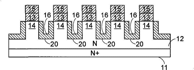
[0032] See figure 2 It is a schematic diagram of a preferred embodiment of a metal oxide semiconductor P-N junction diode structure developed by the present invention to improve the shortcomings of the known technical means. From the figure we can clearly see that the structure of the metal oxide semiconductor PN junction diode 2 mainly includes a substrate 21, a trench structure 22, a gate structure 23, a sidewall structure 24, a metal layer 25, and an ion implantation area. 26. The substrate 21 is composed of a high-doping concentration N-type silicon substrate (N+ silicon substrate) 211 and a low-doping concentration N-type epitaxial layer (N- epitaxial layer) 212, and the trench structure 22 is formed on the substrate 21, the gate structure 23 is formed in the trench structure 22 and protrudes from the surface 2120 of the low doping concentration N-type epitaxial layer 212, and the sidewall structure 24 protrudes from the surface of the substrate 21 and is located at the ga...


PUM


Abstract

The invention discloses a metal oxide semiconductor P-N junction diode and a manufacture method thereof; wherein, the method includes steps as follows: a base plate is provided; a first mask layer is formed on the base plate; first photoetching process is carried out to form a ditch structure on the base plate; first ion implantation process is carried out in the ditch structure; second photoetching process is carried out to form a side wall structure; a second mask layer is formed at the bottom of the ditch structure and on the side wall structure; third photoetching process is carried out to form a grid structure in the ditch structure; second ion implantation process is carried out in the ditch structure; after the removal of a photoresist, third ion implantation process is carried outin the ditch structure; etching process is carried out; a metal layer is formed on the surface of the obtained structure; and fourth photoetching process is carried out to remove partial metal layer.The diode component has high reaction speed, low forward breakover voltage drop value and small reverse bias voltage leakage current.

Description

Technical field [0001] The invention relates to a metal oxide semiconductor P-N junction diode structure and a manufacturing method thereof, in particular to a lower leakage current and lower forward voltage drop value (V F ), a metal oxide semiconductor P-N junction diode structure with higher reverse withstand voltage and low reverse recovery time characteristics. Background technique [0002] The Schottky diode is a unipolar element that uses electrons as carriers. Its characteristics are fast speed and forward conduction voltage drop (V F ) Is low, but the reverse bias leakage current is larger (related to the Schottky barrier value caused by the metal work function and semiconductor doping concentration). The P-N diode is a dual-carrier element that conducts a large amount of current. But the component's forward operating voltage drop value (V F ) Generally higher than the Schottky diode, and the P-N diode has a slower reaction speed and longer reverse recovery time due to t...

Claims


Application Information

Patent Timeline
Patent Type & Authority Patents(China)
IPC IPC(8): H01L21/8249H01L27/095
Inventor 赵国梁郭鸿鑫苏子川
Owner PFC DEVICE
Why Eureka
Try Eureka