Active element array substrate and manufacturing method therefor

A technology of array substrates and active components, applied in semiconductor/solid-state device manufacturing, electrical components, electric solid-state devices, etc., can solve problems affecting photosensitive characteristics, photocurrent attenuation, reduction, etc.

Active Publication Date: 2009-08-19
AU OPTRONICS CORP
View PDF0 Cites 4 Cited by
  • Summary
  • Abstract
  • Description
  • Claims
  • Application Information

AI Technical Summary

Problems solved by technology

However, due to process limitations, the p-i-n photosensor manufactured by LTPS technology will cause poor quantum effect (Quantum Effect, that is, photoelectric conversion efficiency) due to insufficient polysilicon film thickness.
In addition, the light emitted by the backlight will directly irradiate the p-i-n photosensor through the glass substrate, thereby affecting the photosensitive characteristics of the p-i-n photosensor, reducing the signal-to-noise ratio (SNR) of the photosensitive signal and causing distortion of the measurement results
[0005] In other words, the photo-sensing material currently used as the active layer in the photo-sensor faces the following problem: Even if no voltage is applied to the electrodes on both sides of the photo-sensing material, as long as the photo-sensing material is irradiated by light, the photo-sensing The sensor will cause the problem of photocurrent attenuation, which will affect the reliability performance of the photo sensor
As a result, since the patterning process of the light-sensing material is incompatible with the process of the active device array substrate, for the process of the active device array substrate with photosensors, it is necessary to define an additional photomask process. The pattern of light-sensing materials, so the process cannot be effectively reduced to achieve the purpose of saving production costs, resulting in a decline in product competitiveness

Method used


Image

  • Active element array substrate and manufacturing method therefor
  • Active element array substrate and manufacturing method therefor
  • Active element array substrate and manufacturing method therefor

Examples


no. 1 example

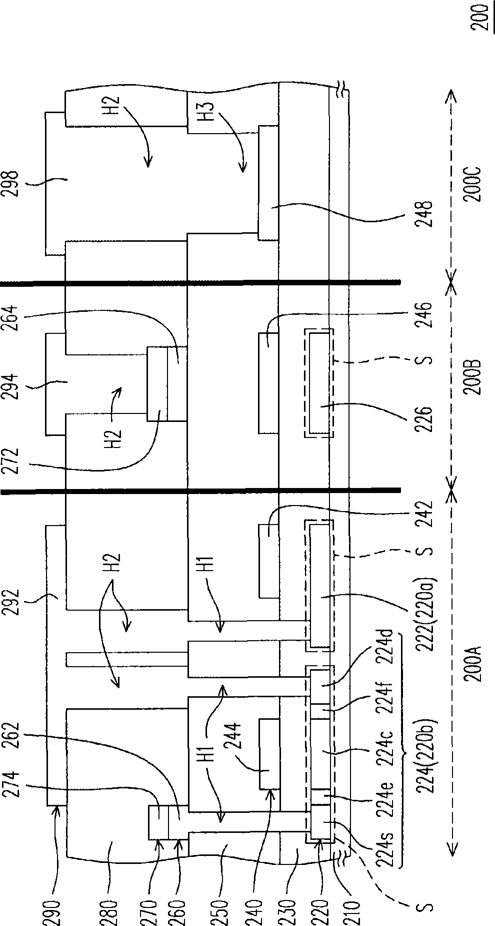
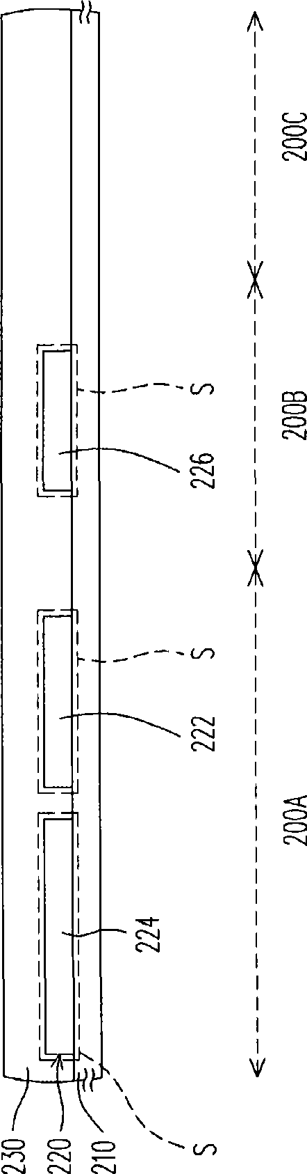
[0123] figure 1 It shows an active device array substrate according to the first embodiment of the present invention, in which, in order to make the diagram expression more concise, there may be a plurality of components in the figure 1 Only one may be shown to represent. Moreover, for the convenience of description, the active element array substrate can be divided into figure 1 The pixel area 200A, the sensing area 200B and the bonding pad area 200C in the. The pixel area 200A has an active element for controlling the display state, and in this embodiment, the active element in the pixel area 200A can be combined with a storage capacitor to provide a better display effect.

[0124] Please refer to figure 1 , the active element array substrate 200 includes a substrate 210, a first patterned semiconductor layer 220, a gate insulating layer 230, a first patterned conductor layer 240, a first dielectric layer 250, a second patterned conductor layer 260, a second patterned Th...

no. 2 example

[0146] image 3 An active device array substrate according to a second embodiment of the present invention is shown. Please refer to image 3 The active device array substrate 300 of this embodiment is similar to the active device array substrate 200 of the first embodiment, but compared with the first embodiment, in the active device array substrate 300 of this embodiment, the pixels located in the pixel area 200A The electrode 292 is indirectly electrically connected to the first patterned semiconductor layer 220 through the first patterned conductor layer 240 and the second patterned conductor layer 260 , for example.

[0147]In detail, compared with the first embodiment, the first patterned conductor layer 240 of the active device array substrate 300 further includes a bridge electrode 249 located in the pixel region 200A. At the same time, the contact conductor 262 of the active device array substrate 300 fills the first contact window H1 and is respectively in contact ...

no. 3 example

[0156] Figure 5 An active device array substrate according to a third embodiment of the present invention is shown. Please refer to Figure 5 The active device array substrate 400 of this embodiment is similar to the active device array substrates 200 and 300 of the foregoing embodiments, but compared with the foregoing embodiments 200 and 300, in the active device array substrate 400 of this embodiment, the pixel area 200A, the third patterned conductor layer 290 serving as the pixel electrode 292 is electrically connected to the first patterned semiconductor layer 220 through some of the second contact windows H2 and the second patterned conductor layer 260 . Moreover, the second patterned semiconductor layer 270 of this embodiment further includes a plurality of pseudo-semiconductor layers 274 located on the contact conductor 262, wherein the size of some of the pseudo-semiconductor layers 274 is, for example, substantially equal to the size of the contact conductor 262, ...


PUM


Abstract

The invention discloses an active component array base plate and a manufacture method thereof, the method comprises the following steps: a first patterned semiconductor layer, a grid insulation layer, a first patterned conductor layer and a first dielectric layer stacked in sequence are formed on a base plate. A plurality of first contact windows exposing the first patterned semiconductor layer are formed on the first dielectric layer and the grid insulation layer. A second patterned conductor layer and a second patterned semiconductor layer on the second patterned conductor are formed on the first dielectric layer. The second patterned conductor layer comprises a plurality of contact conductors and bottom electrodes and the second patterned semiconductor layer comprises an active layer. A second dielectric layer with a plurality of contact windows is formed on the first dielectric layer and the partial second contact windows expose the active layer. A third patterned conductor layer electrically connected with the active layer by the partial contact window is formed on the second dielectric layer.

Description

technical field [0001] The present invention relates to a display array and its manufacturing method, and in particular to an active element array substrate and its manufacturing method. Background technique [0002] With the advancement of technology, the technology of the display is also constantly developing and its demand is increasing day by day. In the early days, due to the excellent display quality and technological maturity of cathode ray tubes (Cathode Ray Tubes, CRTs), they dominated the display market for many years. However, due to the rise of the concept of green environmental protection recently, based on the characteristics of large energy consumption and large radiation generated by cathode ray tubes, and the limited space for flattening their products, cathode ray tubes cannot meet the market demand for light, thin, short , small, beautiful and low power consumption market trends. Therefore, the thin and light flat panel display (Flat Panel Display, FPD) ...

Claims


Application Information

Patent Timeline
Patent Type & Authority Applications(China)
IPC IPC(8): H01L21/84H01L27/14H01L21/027
Inventor 孙铭伟李振岳陈昱丞彭佳添
Owner AU OPTRONICS CORP
Why Eureka
Try Eureka