Sealing structure for processing reaction chamber by semiconductor

A technology of sealed structure and reaction chamber, which is applied in semiconductor/solid-state device manufacturing, pressure vessels used in chemical processes, metal material coating technology, etc., which can solve the problems of sealing ring corrosion, reduced life of sealing ring, and impossibility of complete contact, etc. Problems, to achieve the effect of prolonging life, prolonging path and increasing difficulty

Active Publication Date: 2009-08-26
BEIJING NAURA MICROELECTRONICS EQUIP CO LTD
View PDF0 Cites 14 Cited by
  • Summary
  • Abstract
  • Description
  • Claims
  • Application Information

AI Technical Summary

Problems solved by technology

[0005] The defect of the above-mentioned prior art is that the processing of semiconductor wafers often uses various chemical gases and plasmas, such as figure 2 In the sealing structure shown, the upper and lower sealing surfaces are flat, and it is impossible to completely contact, there will always be a gap, and the gap between the two planes is a straight seam, which allows chemical gases and plasma to pass through this straight seam When in contact with the sealing ring, chemical gases and plasma will corrode the sealing ring, which will reduce the life of the sealing ring and require regular replacement

Method used


Image

  • Sealing structure for processing reaction chamber by semiconductor
  • Sealing structure for processing reaction chamber by semiconductor
  • Sealing structure for processing reaction chamber by semiconductor

Examples


Embodiment Construction

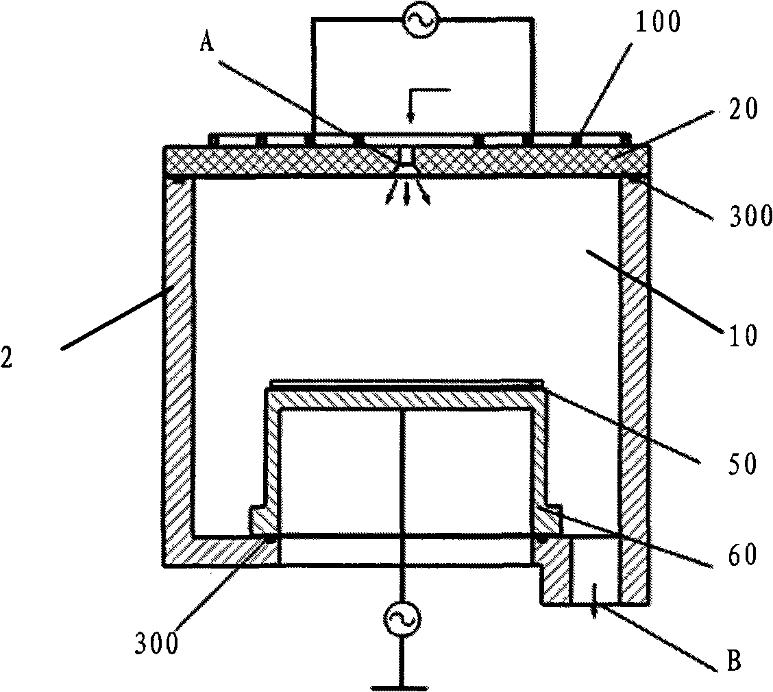
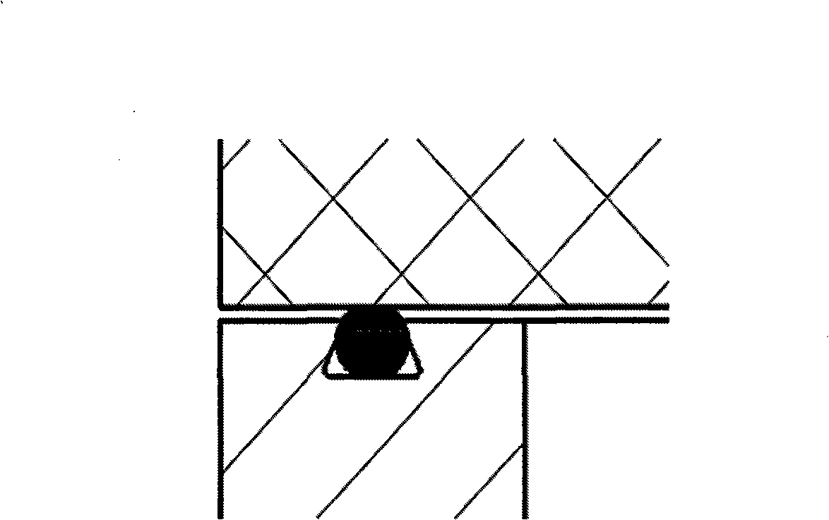
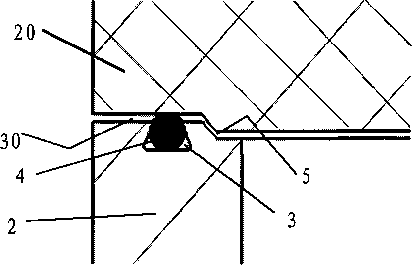
[0024] See 1 and Figure 3 ~ Figure 10 , Which shows a preferred embodiment of a sealing structure for a semiconductor processing reaction chamber of the present invention, including a cover plate 20, a chamber side wall 2 and an electrostatic chuck 60 which are connected to each other and form the reaction chamber 10 together. The connection 30 between the side wall 2 of the chamber and the cover plate 20 and / or the electrostatic chuck 60 is provided with a clamping member 3, usually preferably, at two connections 30 (the connection between the side wall 2 of the chamber and the cover plate 20) The location 30 and the connection location 30) between the side wall 2 of the chamber and the electrostatic chuck 60 are provided with a clamping member 3, which may be a structure that can be used to buckle and fix the sealing member in the prior art, such as a groove or The boss, in this embodiment, is preferably a trapezoidal groove. The clamping member 3 is provided with a sealing memb...


PUM


Abstract

The invention relates to a sealing structure for processing a reaction chamber by semiconductor, which comprises cover plates which are mutually connected and jointly form the reaction chamber, a side wall of the chamber and an electrostatic clamping disc, wherein the joint of the side wall of the chamber and the cover plates and/or electrostatic clamping disc is provided with a clamping piece provided with a sealing piece; and the joint of the side wall of the chamber and the cover plates and/or electrostatic clamping disc is at least provided with a curved surface connecting part, and the inclination angle between the curved surface connecting part and the joint is between 0 and 90 degrees. The length of a gap is lengthened by changing the shape of the gap between the sealing surfaces of the vacuum ends, thereby prolonging the route by which chemical gases and plasmas reach a sealing ring and reducing the amount of the chemical gases and plasmas reaching the sealing ring; and simultaneously, the passing difficulty of the chemical gases and plasmas are greatly increased due to the curved shape, thereby prolonging the service life of the sealing ring.

Description

Technical field [0001] The invention relates to a sealing structure, in particular to a sealing structure used for a semiconductor processing reaction chamber and prolonging the life of a used sealing ring. Background technique [0002] Currently, semiconductor wafer processing is mainly carried out in a vacuum environment. The vacuum environment is realized by pumping the gas in the reaction chamber, and the closed environment of the reaction chamber is realized by the sealing ring. Many chemical gases and plasma devices are used in the processing of semiconductor wafers. Among them, inductively coupled plasma devices are widely used, such as dry etching equipment and chemical vapor deposition. The principle is: Under low pressure, the reaction gas is excited by radio frequency power to generate ionization to form plasma. The plasma is composed of charged electrons and ions. The gas in the reaction chamber is converted into ions under the impact of electrons. In addition, it can...

Claims


Application Information

Patent Timeline
Patent Type & Authority Applications(China)
IPC IPC(8): H01L21/00C23C16/44C23F4/00H01J37/32B01J3/03
Inventor 张风港
Owner BEIJING NAURA MICROELECTRONICS EQUIP CO LTD
Why Eureka
Try Eureka