Thin-film transistor and display device

一种薄膜晶体管、非晶半导体的技术,应用在晶体管、电固体器件、半导体器件等方向,能够解决没确立等问题

Inactive Publication Date: 2009-09-02
SEMICON ENERGY LAB CO LTD
View PDF5 Cites 3 Cited by
  • Summary
  • Abstract
  • Description
  • Claims
  • Application Information

AI Technical Summary

Problems solved by technology

[0012] However, the technology capable of manufacturing high-speed thin-film transistors with high productivity on a large-area mother glass substrate such as the 10th generation (2950mm×3400mm) has not yet been established, which is a problem in the industry

Method used


Image

  • Thin-film transistor and display device
  • Thin-film transistor and display device
  • Thin-film transistor and display device

Examples


Embodiment approach 1

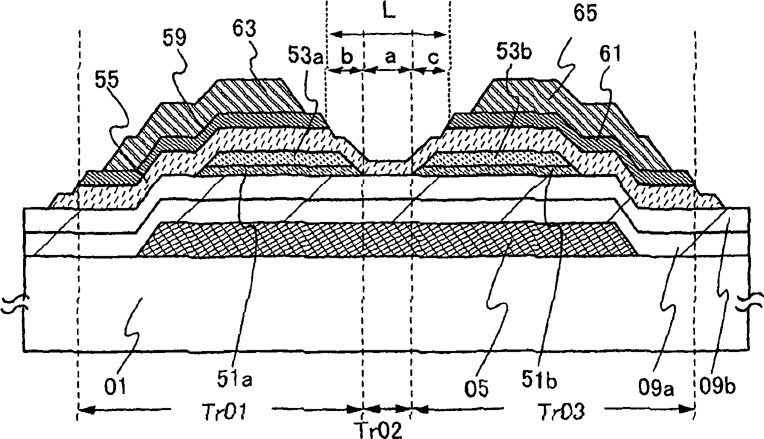
[0057] Here, refer to Figures 1A to 1C The structure of a thin film transistor is described, the cut-off current is lower than that of the thin film transistor with the microcrystalline semiconductor layer in the channel formation region, and its working speed and conduction current are higher than those of the thin film transistor with the amorphous semiconductor layer in the channel formation region.

[0058] exist Figure 1A In the thin film transistor shown, a gate electrode 05 is formed on a substrate 01, gate insulating layers 09a and 09b are formed on the gate electrode 05, and separated conductive layers 51a and 51b are formed on the gate insulating layer 09b. , and separate buffer layers 53a and 53b are formed on the conductive layers 51a and 51b. The buffer layers 53a and 53b substantially overlap the conductive layers 51a and 51b. In addition, an amorphous semiconductor layer 55 covering the side surfaces and upper surfaces of the conductive layers 51a and 51b an...

Embodiment approach 2

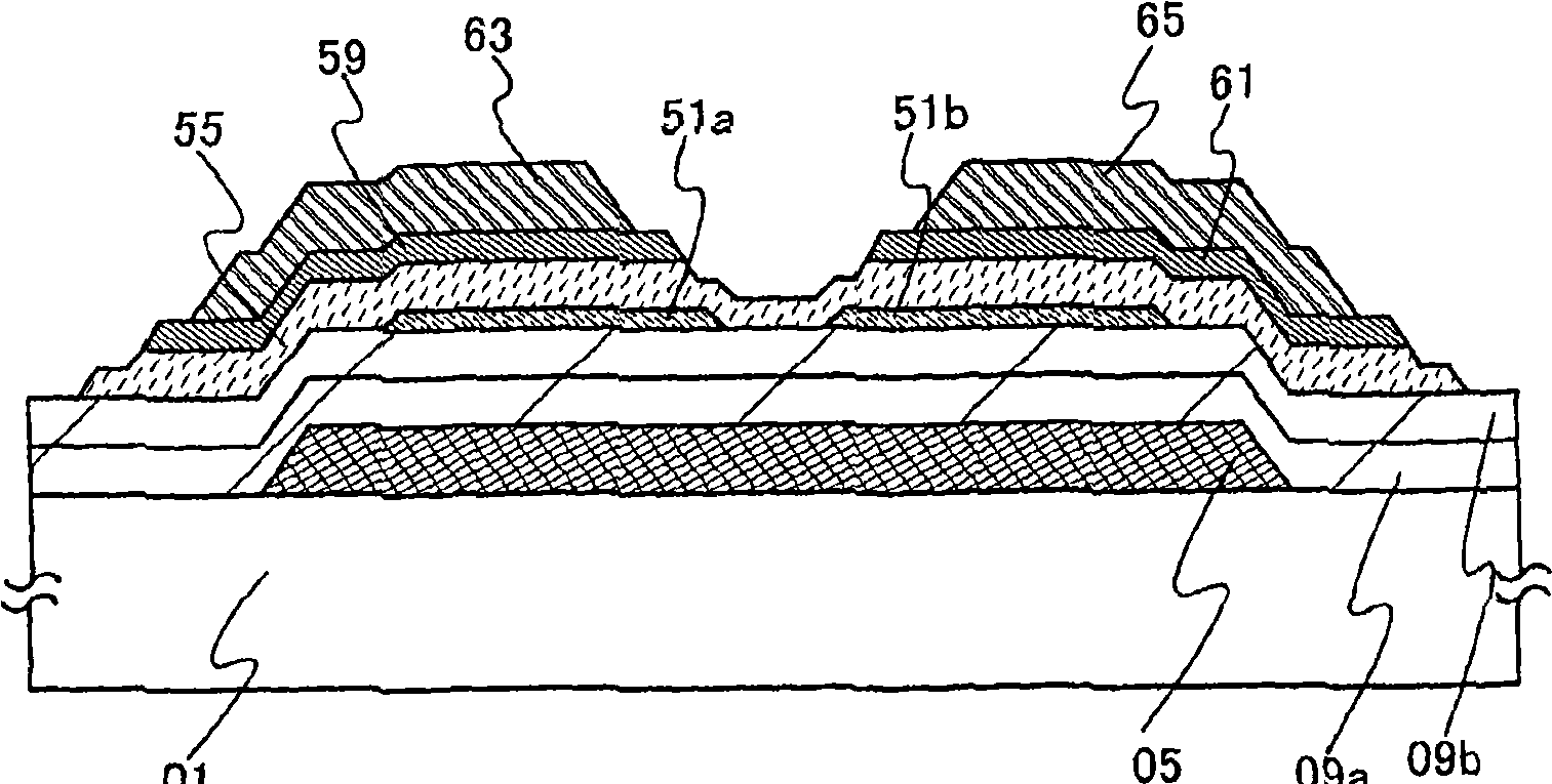
[0102] In this embodiment, refer to figure 2 Other shapes of the conductive layers 51a and 51b and the buffer layers 53a and 53b are shown.

[0103] figure 2 The shown thin film transistor is a thin film transistor in which the buffer layers 53c and 53d are respectively formed inside the separated conductive layers 51c and 51d in its cross-sectional structure, that is, the buffer layers 53c and 53d are formed with an area smaller than that of the conductive layers 51c and 51d. And the thin film transistors of the conductive layers 51c and 51d are partially exposed from the buffer layers 53c and 53d. By adopting this structure, when the conductive layers 51c and 51d are microcrystalline semiconductor layers, metal silicide layers or metal layers, the contact conduction can be improved by using the microcrystalline semiconductor layers, metal silicide layers or metal layers as crystal growth nuclei. The crystallinity of the amorphous semiconductor layer 55 of the layers 51c ...

Embodiment approach 3

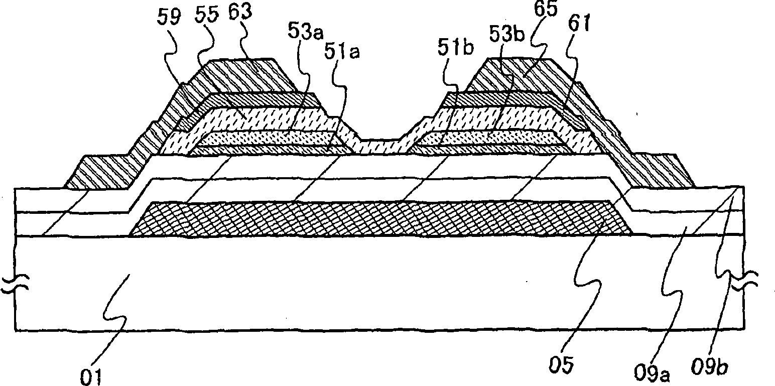
[0107] In this embodiment, refer to Figure 3A and 3B Other ways of showing buffer layers. The present embodiment is characterized in that the buffer layers 52a and 52b are formed of insulating layers.

[0108] exist Figure 3A In the thin film transistor shown, a gate electrode 05 is formed on a substrate 01, gate insulating layers 09a and 09b are formed on the gate electrode 05, and separated conductive layers 51a and 51b are formed on the gate insulating layer 09b. , and separate buffer layers 52a and 52b are formed on the conductive layers 51a and 51b. The buffer layers 52a and 52b substantially overlap the conductive layers 51a and 51b. Furthermore, an amorphous semiconductor layer 55 is formed to cover the side surfaces and upper surfaces of the conductive layers 51a and 51b and the buffer layers 52a and 52b. A pair of impurity semiconductor layers 59 and 61 to which an impurity element imparting one conductivity type is added is formed on the amorphous semiconducto...


PUM

PropertyMeasurementUnit
electrical conductivityaaaaaaaaaa
particle diameteraaaaaaaaaa

Abstract

A thin-film transistor includes a pair of impurity semiconductor layers in which an impurity element imparting one conductivity type is added to form a source and drain regions so as to be overlapped at least partly with a gate electrode with a gate insulating layer interposed between the gate electrode and the impurity semiconductor layers; a pair of conductive layers which is overlapped over thegate insulating layers at least partly with the gate electrode and the impurity semiconductor layers, and is disposed with a space therebetween in a channel length direction; and an amorphous semiconductor layer which is in contact with the gate insulating layer and the pair of conductive layers and is extended between the pair of conductive layers.

Description

technical field [0001] It relates to a thin film transistor or a display device using the thin film transistor. Background technique [0002] As one type of field effect transistor, a thin film transistor in which a channel formation region is formed in a semiconductor layer formed on a substrate having an insulating surface is known. Technologies using amorphous silicon, microcrystalline silicon, and polycrystalline silicon as semiconductor layers for thin film transistors have been disclosed (see Patent Documents 1 to 5). A typical application example of a thin film transistor is a liquid crystal television device, and it is put into practical use as a switching transistor constituting each pixel of a display panel. [0003] Patent Document 1 Japanese Patent Application Publication No. 2001-053283 [0004] Patent Document 2 Japanese Patent Application Publication No. H5-129608 [0005] Patent Document 3 Japanese Patent Application Publication No. 2005-049832 [0006] P...

Claims


Application Information

Patent Timeline
Patent Type & Authority Applications(China)
IPC IPC(8): H01L29/78H01L29/36H01L27/12H01L21/20H01L21/265G02F1/1362G02F1/1345G02F1/1368H01L29/417H01L29/423H01L29/49H01L29/786
CPCH01L29/4908H01L27/1288H01L29/458H01L29/04H01L29/66765H01L27/1214
Inventor 大力浩二宫入秀和黑川义元山崎舜平乡户宏充河江大辅小林聪
Owner SEMICON ENERGY LAB CO LTD
Why Eureka
Try Eureka