
Manufacturing method of circuit board with selectively plated copper and tin

A technology of electroplating copper and circuit boards, which is applied in the manufacture of printed circuits, the removal of conductive materials by chemical/electrolytic methods, printed circuits, etc., can solve the problems of waste of precious metal chemical materials, increase production costs, environmental pollution, etc., and achieve cleanliness The effect of production, pollution reduction and production cost reduction

Inactive Publication Date: 2011-04-06
深圳市源基电子科技有限公司 +1
View PDF0 Cites 0 Cited by
  • Summary
  • Abstract
  • Description
  • Claims
  • Application Information

AI Technical Summary

Problems solved by technology

It can be seen that the traditional process not only causes serious environmental pollution, but also causes a lot of waste of precious metals, water, electricity, and chemical materials, which greatly increases the production cost of enterprises.

Method used

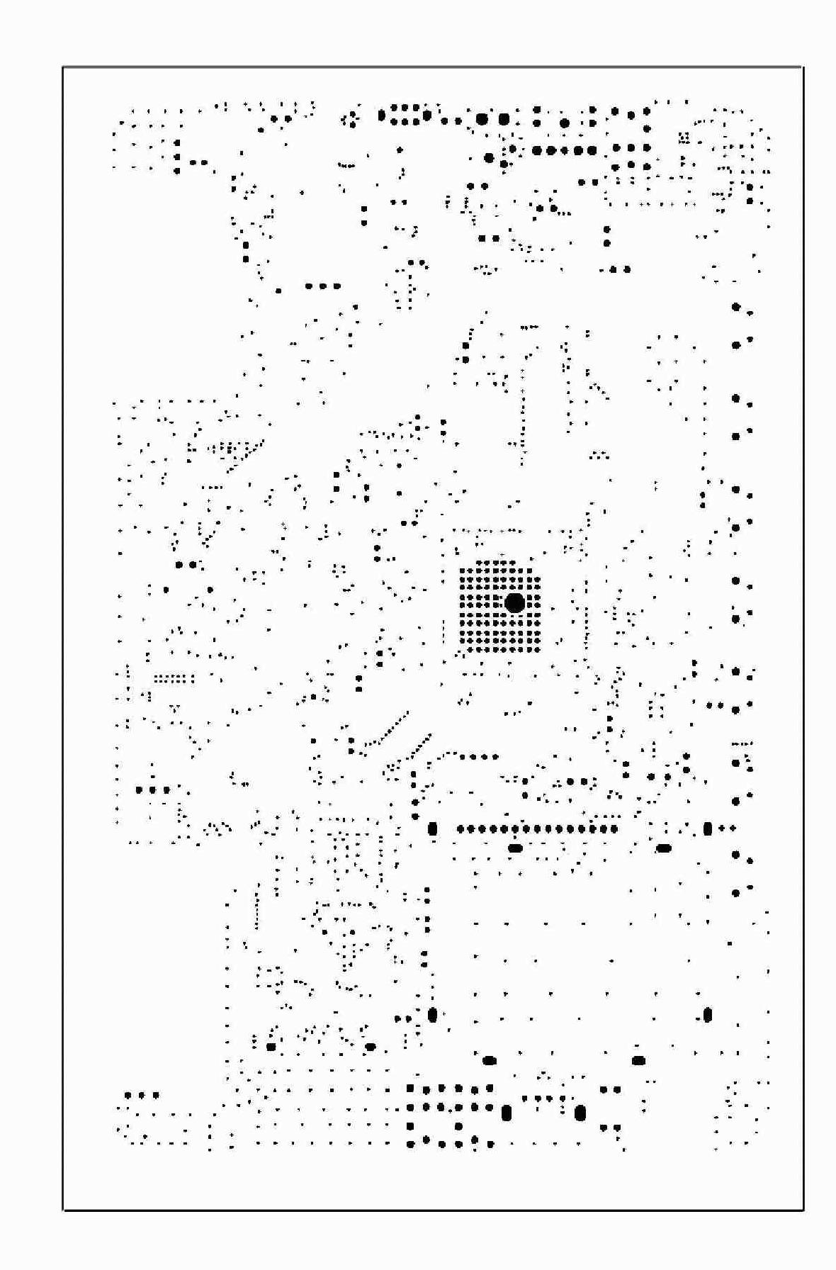
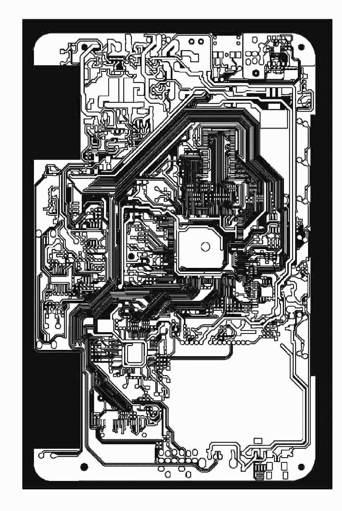
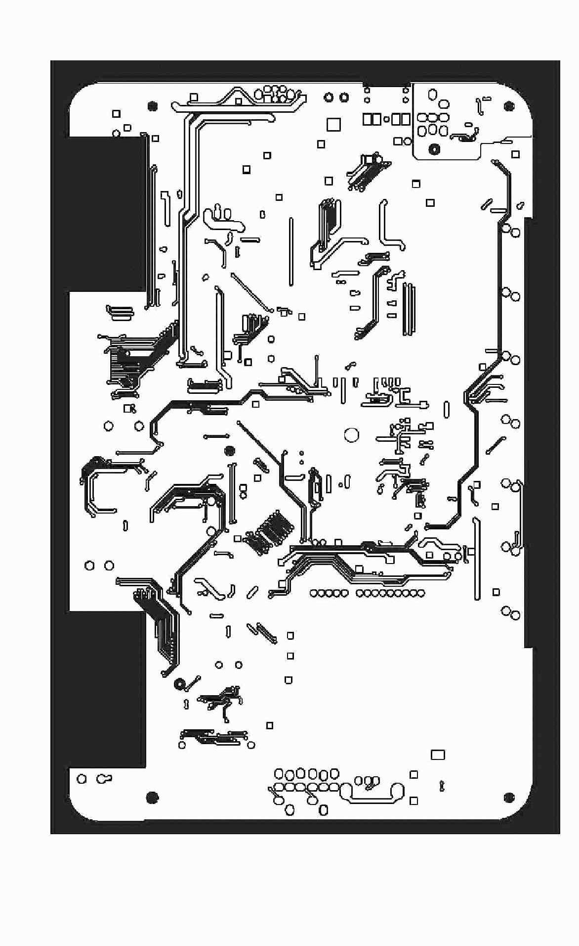

Image

  • Manufacturing method of circuit board with selectively plated copper and tin
  • Manufacturing method of circuit board with selectively plated copper and tin
  • Manufacturing method of circuit board with selectively plated copper and tin

Examples


Embodiment Construction

[0016] The following examples are further explanations and illustrations of the present invention, and do not constitute any limitation to the present invention.

[0017] The manufacturing method of the circuit board of electroplating copper, tin selectively of the present invention (taking double panel as example), the steps are as follows:

[0018] First, drill holes on the cut and baked copper clad board according to the program compiled by the user, and then perform copper sinking or first copper plating on the drilled holes to make the circuits on both sides of the copper clad board conductive. This step is different from the conventional one. The method is similar.

[0019] The gist of the present invention is to selectively electroplate copper and tin on the circuit pattern to replace large-area electroplating copper and tin on the circuit board. The specific steps are:

[0020] 1. Coating a layer of anti-plating covering film on the circuit board after sinking copper ...


PUM


Abstract

The invention relates to a manufacturing method of a circuit board with selectively plated copper and tin, comprising the following steps: coating a plating-resistant cover film on a copper precipitatThe invention relates to a manufacturing method of a circuit board with selectively plated copper and tin, comprising the following steps: coating a plating-resistant cover film on a copper precipitation circuit board or a circuit board plated with copper at first time, and then bonding positive sheets of all metal holes and hole rings, which are contained in circuit diagrams, on the plating-resision circuit board or a circuit board plated with copper at first time, and then bonding positive sheets of all metal holes and hole rings, which are contained in circuit diagrams, on the plating-resistant cover film to form a primary circuit after exposure and development; plating copper and tin on the hole walls of all the metal holes and the hole rings and then carrying out film de-coating; coattant cover film to form a primary circuit after exposure and development; plating copper and tin on the hole walls of all the metal holes and the hole rings and then carrying out film de-coating; coating a corrosion-resistant cover film on the de-coated circuit board, and then bonding negative sheets of the circuit diagrams on the corrosion-resistant cover film to form a secondary circuit after exing a corrosion-resistant cover film on the de-coated circuit board, and then bonding negative sheets of the circuit diagrams on the corrosion-resistant cover film to form a secondary circuit after exposure and development; etching the circuit diagrams and then carrying out film de-coating and tin de-coating; and manufacturing a circuit board product after welding prevention, exposure, developmentposure and development; etching the circuit diagrams and then carrying out film de-coating and tin de-coating; and manufacturing a circuit board product after welding prevention, exposure, development, element mark printing, tin spraying, anti-oxidation process or turmeric and outline process. The invention selectively plates copper and tin, thereby greatly reducing the amount of copper and tin to, element mark printing, tin spraying, anti-oxidation process or turmeric and outline process. The invention selectively plates copper and tin, thereby greatly reducing the amount of copper and tin togreatly reduce the environmental pollution from tin de-coating process, effectively saving the copper, tin, water, electricity, chemical materials, energy charges and manpower and effectively reducin greatly reduce the environmental pollution from tin de-coating process, effectively saving the copper, tin, water, electricity, chemical materials, energy charges and manpower and effectively reducing the production costs for enterprises.g the production costs for enterprises.

Description

【Technical field】 [0001] The present invention relates to a printed circuit board (PCB), particularly relates to a kind of electroplating and stripping tin selectively on the printed circuit board, which can greatly reduce the plated area of ​​copper and tin to about 90%, thus effectively saving copper, A method for making a circuit board with the amount of precious metals such as tin. 【Background technique】 [0002] As we all know, printed circuit boards (PCBs) are widely used as the basic material of the electronics industry. As small as electronic watches, calculators, personal computers, as large as computers, communication equipment, medical equipment, and aerospace or military equipment, as long as there are electronic components such as integrated circuits, PCBs are used for electrical interconnection between them. Printed circuit boards are formed by setting conductive patterns for electrical connections between electronic components on an insulating substrate, and ...

Claims


Application Information

Patent Timeline
Patent Type & Authority Patents(China)
IPC IPC(8): H05K3/00H05K3/06H05K3/42
Inventor 陈国富
Owner 深圳市源基电子科技有限公司
Learn More