Image sensor capable of reducing noise

An image sensor and noise technology, applied in image communication, electrical solid-state devices, semiconductor devices, etc., can solve the problems of limited use of metal blocks and the inability of photoresist to completely and effectively isolate light

Inactive Publication Date: 2009-09-09
NOVATEK MICROELECTRONICS CORP
View PDF0 Cites 4 Cited by
  • Summary
  • Abstract
  • Description
  • Claims
  • Application Information

AI Technical Summary

Problems solved by technology

However, the photoresist cannot completely and effectively isolate the light, and under the consideration

Method used


Image

  • Image sensor capable of reducing noise
  • Image sensor capable of reducing noise
  • Image sensor capable of reducing noise

Examples


Embodiment Construction

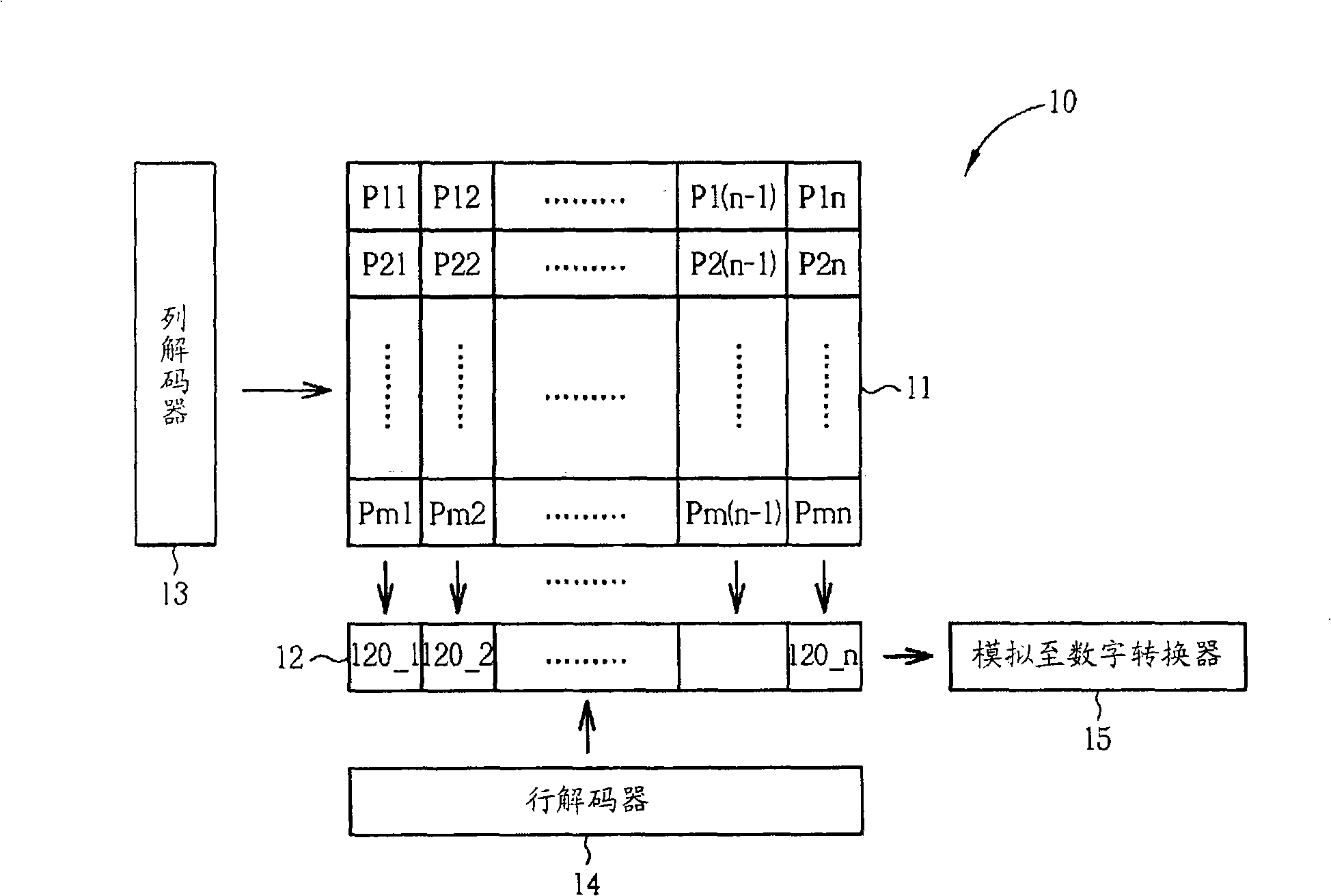
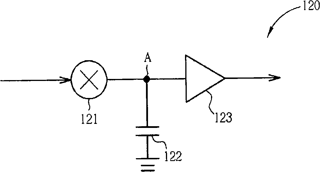
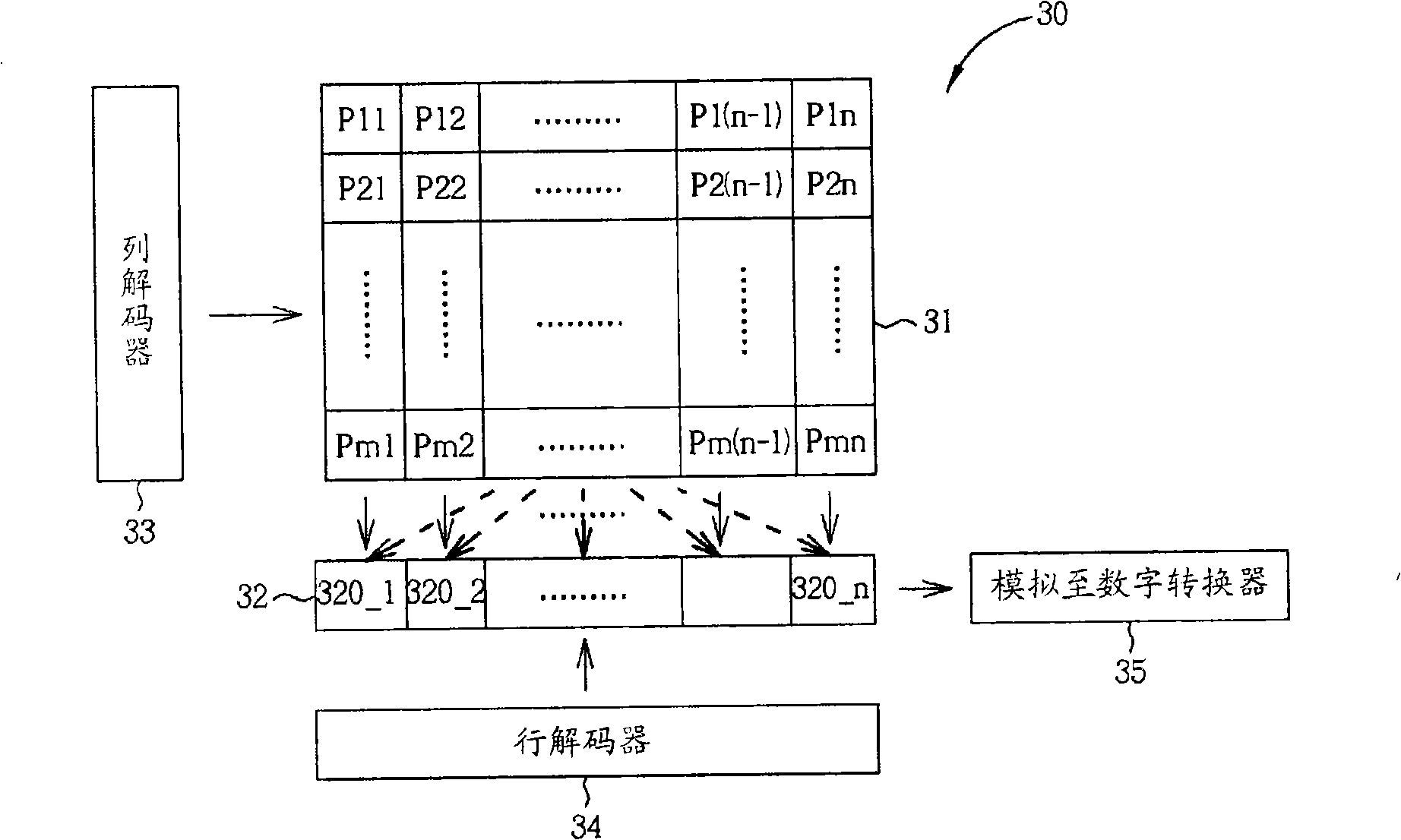
[0042] Please refer to image 3 , image 3 It is a schematic diagram of a CMOS image sensor 30 of the present invention. The CMOS image sensor 30 includes a pixel array 31 , a correlated double sampling (Correlation Double Sampling, CDS) circuit array 32 , a column decoder 33 , a row decoder 34 and an analog-to-digital converter 35 . Wherein pixel array 31, column decoder 33, row decoder 34 and analog-to-digital converter 35 and figure 1 The CMOS image sensor 10 is similar to the middle CMOS image sensor and will not be repeated here. The associated double sampling circuit array 32 is arranged on the lower side of the pixel array 11, and is composed of associated double sampling circuits 320_1-320_n, and the internal circuit of each associated double sampling circuit is connected with figure 2 The correlated double sampling circuit 120 shown is similar and will not be repeated here. Since each associated double sampling circuit 320 has a different position in the associat...


PUM


Abstract

An image sensor capable of reducing noise comprises a pixel array, a control circuit and an associative double sampling circuit array. The associative double sampling circuit array is coupled between the pixel array and the control circuit and consists of a plurality of associative double sampling circuit units, wherein each associative double sampling circuit unit comprises a silicon substrate, an MOS element which is formed on the silicon substrate and connected to a floating connection point of the associative double sampling circuit, and a plurality of metal layers which are arranged on the MOS element for providing the electric connection of the associative double sampling circuit unit and protecting the MOS element from light irradiation.

Description

technical field [0001] The present invention relates to an image sensor capable of reducing noise, and in particular to a metal connecting wire provided for electrically connecting each circuit node in an associated double sampling circuit to block light from irradiating the voltage in the associated double sampling circuit. Floating nodes, thereby avoiding noise generation of CMOS image sensors. Background technique [0002] With the continuous development and growth of electronic products such as digital cameras and mobile phones, the demand for image sensing components in the consumer market continues to increase. Generally speaking, currently commonly used image sensing devices include charge coupled sensing devices <Charge Coupled Device, CCD> and complementary metal oxide semiconductor image sensing devices <CMOS Image Sensor, CIS> two categories. Among them, due to the characteristics of low operating voltage, low power consumption and high operating effi...

Claims


Application Information

Patent Timeline
IPC IPC(8): H01L27/146H01L23/522H04N3/15H04N5/217H04N5/357H04N5/374H04N5/378
Inventor 詹日维
Owner NOVATEK MICROELECTRONICS CORP
Why Eureka
Try Eureka