Photonic crystal wavelength division multiplexer and design method thereof

A technology of wavelength division multiplexing devices and photonic crystals, applied in optical components, light guides, optics, etc., can solve the problems of low integration, low Q value, high integration, etc., and achieve the effect of high integration and small volume

Inactive Publication Date: 2009-09-16
SUN YAT SEN UNIV
View PDF0 Cites 19 Cited by
  • Summary
  • Abstract
  • Description
  • Claims
  • Application Information

AI Technical Summary

Problems solved by technology

[0005] In order to solve the technical problems such as low Q value, low integration and difficulty in manufacturing existing single resonant cavity structure wavelength division multiplexing devices, the primary purpose of the present invention is to provide a design method for photonic crystal wavelength division multiplexing devices ; This method is easy to implement, and the designed wavelength division multiplexing device has the advantages of high Q value and high integration

Method used


Image

  • Photonic crystal wavelength division multiplexer and design method thereof
  • Photonic crystal wavelength division multiplexer and design method thereof
  • Photonic crystal wavelength division multiplexer and design method thereof

Examples


Embodiment 1

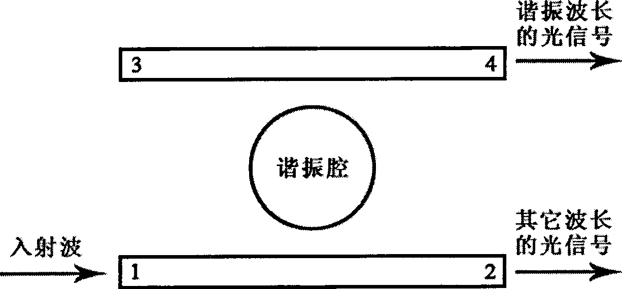
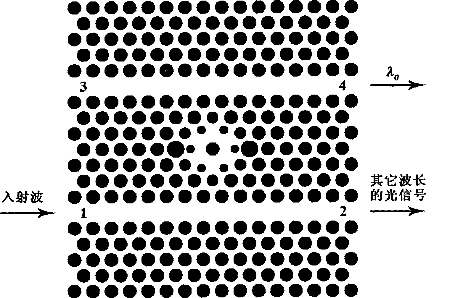
[0043] Figure 6 Shown is a wave division multiplexer with two download / upload channels obtained according to the design method of the present invention. Figure 6 In the shown light wave demultiplexing device, the lattice constant is a=0.45 μm, and the radius of the air column is r=0.35a. The structural parameter of the first resonant cavity R1 is r O1 =0.35a, r A1 =0.21a, r d1 = 1.21a, r B1 =0.30a, r C1 =0.46a. The structural parameter of the second resonator R2 is r O2 =0.35a, r A2 =0.21a, r d2 = 1.21a, r B2 =0.30a, r C2 =0.46a. The structures of the two resonant cavities R1 and R2 are the same: the air columns are arranged in the same structure, and the lattice constants are also equal. At this time, the operating wavelengths of the two resonators R1 and R2 are λ 1 = 1556.3nm and λ 2 = 1572.8nm. The first waveguide 1-2 is a linear waveguide, used as an input waveguide, and is the channel main line; the second waveguide 3-4 and the third waveguide 5-6 are zig...

Embodiment 2

[0047] Figure 8 Also shown is a WDM multiplexer with two download channels, with Figure 6 The difference is that the lattice constants of the air column arrays on both sides of the dotted line are different. Lattice constant a on the left 1 =0.445μm, the right lattice constant a 2 =0.45μm, the air column radii on the left and right sides are r 1 =0.35a 1 , r 2 =0.35a 2 . The structural parameters of the two resonant cavities are as follows: the structural parameters of the third resonant cavity R3 are r O3 =0.35a 1 , r A3 =0.21a 1 , r d3 =1.21a 1 , r B3 =0.30a 1 , r C3 =0.46a 1 ; The structural parameter of the fourth resonant cavity R4 is r O4 =0.35a 2 , r A4 =0.20a 2 , r d4 =1.20a 2 , r B4 =0.25a 2 , r C4 =0.46a 2. It can be seen that each structural parameter of the third resonant cavity R3 is related to a 1 The ratio of and each structural parameter of the fourth resonant cavity R4 and a 2 The ratios are equal; that is, the two resonant cavit...

Embodiment 3

[0049] Figure 10 It is a schematic diagram of an 8-way wave division multiplexer, the solid line represents the photonic crystal waveguide, and the circle represents the resonant cavity structure in the present invention. Each resonator (R5, R6, R7, ..., R12) can use the method of embodiment 1 or embodiment 2 to adjust the resonance wavelength (respectively λ 5 ,λ 6 ,λ 7 ,...,λ 12 ), so that the signal of the corresponding wavelength on the main line is separated to each download channel for output. As can be seen above, see Figure 10 The arrangement of the resonant cavity and the waveguide can produce a wave division multiplexer with any number of download channels; Figure 10 The device can also perform inverse process processing on the optical signal to realize the wavelength division multiplexer function of any number of upload channels.


PUM


Abstract

The invention relates to a photonic crystal wavelength division multiplexer and a design method thereof. The design method comprises the following steps: (1) a cylindrical air column with radius of r arranged in triangular lattice is introduced into a two-dimensional plate composed of waveguide materials to form a two-dimensional photonic crystal; (2) the air columns on at least two lines are removed from the two-dimensional plate so as to form at least two linear defects, an input waveguide and at least an output waveguide, and air columns of odd-numbered lines not less than 7 are reserved between the input waveguide and the output waveguide; (3) resonant cavities with resonant modes in odd and even symmetry are constructed in the reserved air columns. The operating wavelength can be adjusted by changing structural parameters or lattice constants of the resonant cavities; wavelength division multiplexers with arbitrary multi-path download channel number can be manufactured by arranging certain resonant cavities and wave guides. The download bandwidth of the invention is less than 0.5nm and can be applied to dense wavelength division multiplex systems with wavelength interval standard of 0.8nm.

Description

technical field [0001] The invention relates to a wavelength division multiplexing device technology in the optical band, in particular to a photonic crystal wavelength division multiplexing device suitable for 1550nm wave band and a design method thereof. Background technique [0002] In optical fiber communication, wavelength division multiplexing (WDM) technology is a commonly used multiplexing technology, which is a technology for simultaneously transmitting multiple wavelength optical signals in one optical fiber. The wavelength division multiplexing equipment is used to modulate the signals of different channels into light of different wavelengths, and multiplex them to the optical fiber channel, so as to realize the expansion of the network. The expansion effect of wavelength division multiplexing technology is remarkable, and it is relatively easy and convenient in network deployment, so it has become the focus of optical communication development. [0003] Photonic...

Claims


Application Information

Patent Timeline
Patent Type & Authority Applications(China)
IPC IPC(8): G02B6/122
Inventor 金崇君赵铱楠
Owner SUN YAT SEN UNIV
Why Eureka
Try Eureka