MBE epitaxial method for positioning and growing low-intensity InAs quantum dot by strain engineering theory and pattern-underlay combining technology

A graphic substrate and strain engineering technology, applied in ion implantation plating, metal material coating process, coating, etc., can solve problems such as difficulty in obtaining microcavity structure and difficulty in single photon emitting devices

Inactive Publication Date: 2009-09-16
CHANGCHUN UNIV OF SCI & TECH
View PDF0 Cites 10 Cited by
  • Summary
  • Abstract
  • Description
  • Claims
  • Application Information

AI Technical Summary

Problems solved by technology

However, due to the lack of high reflectivity distributed Bragg reflectors (DBR) in the InP-based material system, it is difficult to obtain a microcavity structure, which leads to certain difficulties in realizing practical single-photon emission devices using InAs / InP quantum dots.

Method used


Image

  • MBE epitaxial method for positioning and growing low-intensity InAs quantum dot by strain engineering theory and pattern-underlay combining technology
  • MBE epitaxial method for positioning and growing low-intensity InAs quantum dot by strain engineering theory and pattern-underlay combining technology

Examples


Embodiment Construction

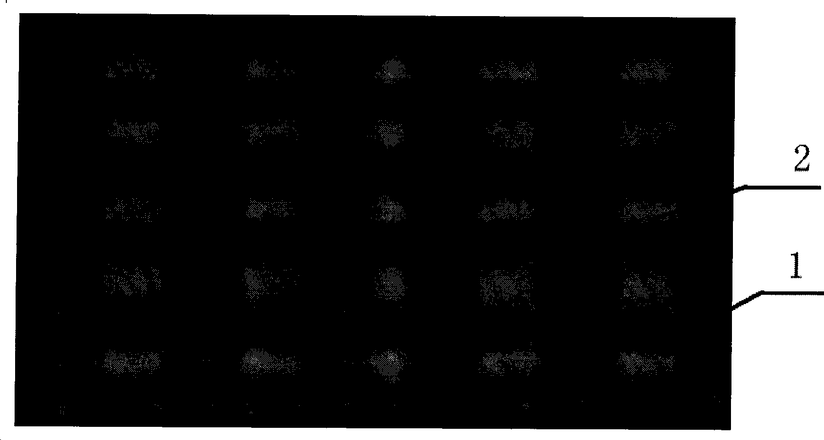
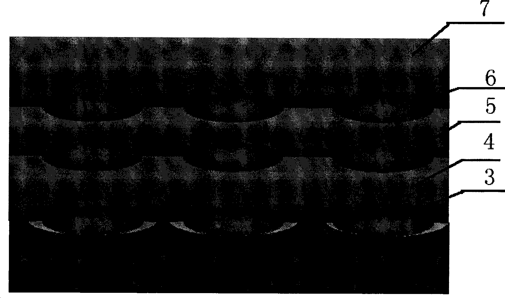
[0010] The invention is an MBE epitaxy method for positioning and growing low-density InAs quantum dots by adopting strain engineering principle and graphic substrate combination technology. Combination hint figure 1 and figure 2 illustrate:

[0011] 1. Using electron beam lithography (EBL) combined with wet / dry etching technology to prepare the required pattern (2) on the GaAs substrate wafer (1):

[0012] A. Choose EBL exposure time 50-65s;

[0013] B. H3PO 3 : H2O 2 :H 2 O is used as the corrosion solution, the corrosion temperature is 0°C, and the corrosion time is 3-5 minutes;

[0014] C. In order to control the pattern size, pattern spacing and corrosion depth of mesa / pit, dry etching uses Cl 2 、BCl 3 For etching gas, control the etching time to 2-4min;

[0015] 2. On the basis of successfully preparing the required pattern substrate, epitaxially grow the seed quantum dot layer (3);

[0016] Control the growth temperature of the seed quantum dot layer at 540°C...


PUM

PropertyMeasurementUnit
thicknessaaaaaaaaaa
temperatureaaaaaaaaaa
thicknessaaaaaaaaaa

Abstract

Single photon is realized by the luminescence of a single quantum dot under ideal condition, so that the effective insulation of the single quantum dot becomes very important. At present, InAs/GaAs quantum dots which are used for manufacturing and realizing a quantum dot single photon emission apparatus are obtained by a self-organized growth method, the InAs/GaAs quantum dots are distributed on a growth surface at random and have very high dot density, and several to hundreds of quantum dots are distributed on every square micron, so that the effective insulation of the single quantum dot is comparatively difficult. Due to the randomicity of the distribution of the quantum dots on the growth surface, the positions of the quantum dots in an optical microcavity become very hard to be controlled reliably. The invention prepares low-intensity InAs quantum dots by means of combining a strain engineering theory with a pattern underlay. The strain engineering theory is as follows: during the process of growing multilayer quantum dots, stress field action is produced due to the existence of underlayer quantum dots, and upper layer dots in the multilayer quantum dots tend to keep growing on the same position with the underlayer quantum dots in the vertical direction to form vertical matching. In addition, the optical quality for growing the quantum dots on the pattern underlay can be improved effectively just by a lamina GaAs cushion layer with the thickness of tens of nanometers. The invention provides an MBE epitaxial method for positioning and growing a low-intensity InAs quanta dot by a strain engineering theory and a pattern-underlay combining technology, thus overcoming the randomicity for growing the quanta dot by the self-organized growth method and controlling the position and the density reliably. The method provides a reference measure for a method for preparing a quanta dot single photon emission source.

Description

technical field [0001] The invention relates to the epitaxial growth technology of semiconductor light-emitting materials, and belongs to the technical field of semiconductor material epitaxial growth. Background technique [0002] Due to the strong three-dimensional quantum confinement, quantum dots have unique atom-like properties, so they have a strong ability to emit single photons. Especially self-organized semiconductor quantum dots, which have good structural and optical stability, high radiation recombination efficiency, can reliably generate single photons, are easy to integrate with microcavities, can achieve electrical injection, and are easy to package and even realize commercialization. And so on, so it becomes one of the most ideal candidate materials to realize practical single-photon emitting devices. In the past ten years, the research and development of semiconductor quantum dot single-photon emission sources has become an international frontier and hot sp...

Claims


Application Information

Patent Timeline
Patent Type & Authority Applications(China)
IPC IPC(8): H01L21/203H01L21/302H01L33/00C23C14/22C23C14/02
Inventor 刘国军李联合李占国李林李梅尤明慧芦鹏李辉乔忠良高欣曲轶
Owner CHANGCHUN UNIV OF SCI & TECH
Why Eureka
Try Eureka