

Surface metallised ceramic and manufacturing method thereof
A technology for metallization and ceramics, applied in the field of surface metallization ceramics and its manufacturing, can solve the problems of inaccessibility of molten aluminum, inability to make films, non-wetting, etc., and achieve the effect of good physical and mechanical properties
- Summary
- Abstract
- Description
- Claims
- Application Information
AI Technical Summary
Problems solved by technology
Method used
Image

Examples
Embodiment 1
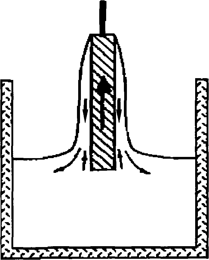
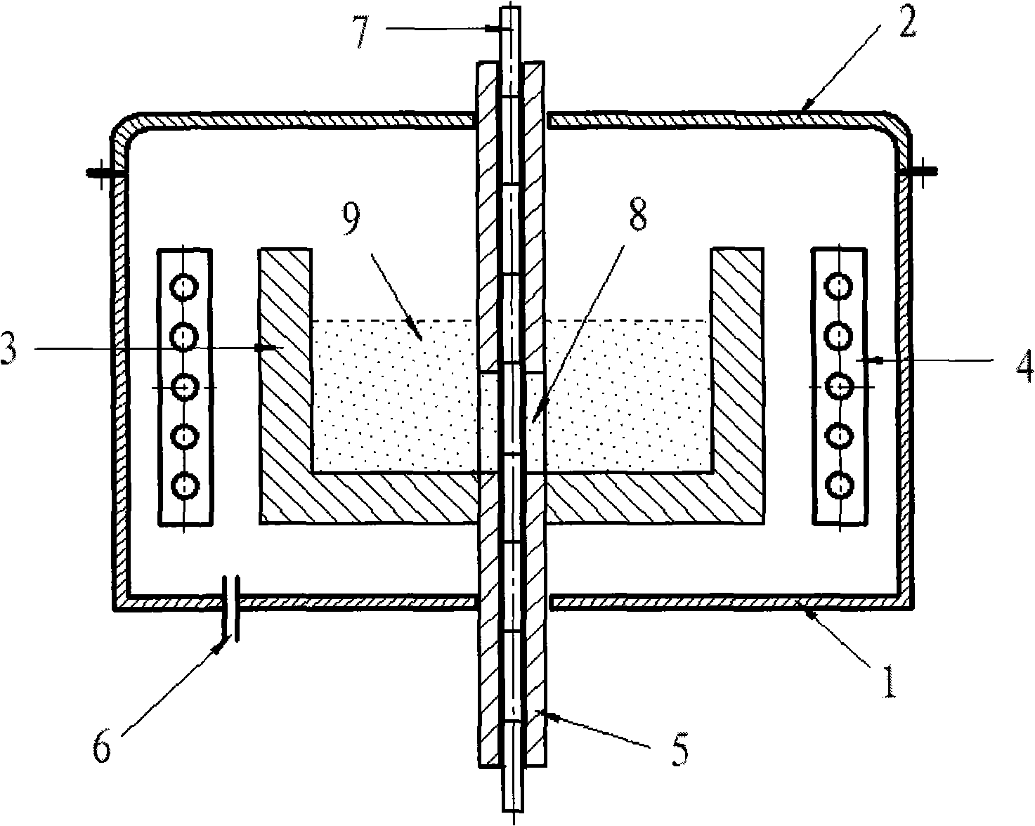
[0028] Embodiment 1, adopt above-mentioned ceramic surface metallization device, put pure aluminum (99.9%) into graphite crucible, alumina ceramic plate (long 137mm, wide 35mm, thick 0.64mm, produced by Tsinghua Yueke, the purity of alumina is greater than 95 %) into the graphite guide rail passing through the crucible, and then heated in a nitrogen atmosphere (nitrogen flow rate is 20 liters / min) to melt the aluminum and raise the temperature to 730°C. Insert another alumina ceramic plate into the guide rail at a speed of 68.5mm / min from the guide rail entrance at the lower part of the device, and push the ceramic plate inserted into the guide rail to move vertically upward at the same speed. During the moving process, the ceramic plate contacts the aluminum melt in the crucible through the window on the guide rail, and then pushes out from the upper part of the guide rail together with the aluminum melt adhered to the surface, cools, and forms a thickness of about 6 microns o...
Embodiment 2
[0031] Embodiment 2, except that the melt temperature is reduced to 700° C., is the same as embodiment 1. Form a dense aluminum film with an average thickness of 7 microns on the surface of the ceramics by this method, and the stripping rate of the adhesive tape test is 0. The experiment was repeated 3 times with the same results.
Embodiment 3
[0032] Embodiment 3, except that the melt temperature is increased to 760° C., is the same as embodiment 1. This method is used to form a dense aluminum film with an average thickness of 5 microns on the surface of the ceramics, and its tape test peeling rate is 0. The experiment was repeated 3 times with the same results.
PUM
| Property | Measurement | Unit |
|---|---|---|
| The average thickness | aaaaa | aaaaa |
| The average thickness | aaaaa | aaaaa |
| The average thickness | aaaaa | aaaaa |
Abstract
Description
Claims
Application Information