Metal-semiconductor field effect transistor and production method thereof

A field-effect transistor and manufacturing method technology, applied in the manufacture of high-frequency and high-power integrated circuits, the field-effect transistor field, can solve the problems of reduced leakage current, reduced electron mobility, trap effect, etc., so as to reduce the contact area, improve the Control ability, the effect of reducing the impact

Inactive Publication Date: 2009-10-07
XIDIAN UNIV
View PDF0 Cites 4 Cited by
  • Summary
  • Abstract
  • Description
  • Claims
  • Application Information

AI Technical Summary

Problems solved by technology

[0013] However, due to the serious trap effect on the surface of the existing MESFET device structure, when the MESFET device is biased by the drain voltage, electrons are trapped by surface traps when they tunnel from the gate to the surface charge depletion region. In turn, a parasitic gate is generated near the surface and a depletion layer is formed
This depletion layer will result in a reduction in the effective channel thickness, a decrease in electron mobility, and a decrease in leakage current
With the increase of the gate-drain voltage difference, the influence of the surface trap effect becomes more obvious, which will seriously affect the microwave power output characteristics of the MESFET

Method used


Image

  • Metal-semiconductor field effect transistor and production method thereof
  • Metal-semiconductor field effect transistor and production method thereof
  • Metal-semiconductor field effect transistor and production method thereof

Examples


Embodiment 1

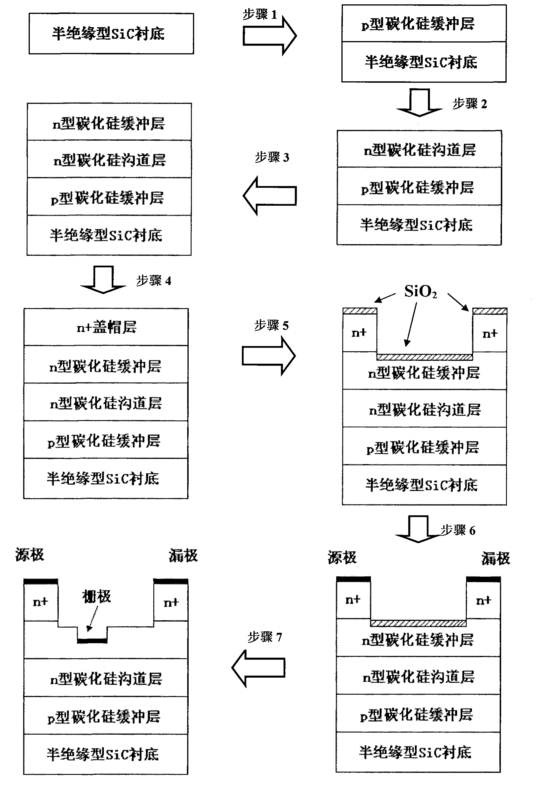
[0030] Embodiment 1, the specific process of making the device of the present invention is as follows:

[0031] Step 1, epitaxially growing a p-type silicon carbide buffer layer.

[0032] On a semi-insulating silicon carbide substrate, a layer of p-type doping is epitaxially grown with a concentration of 1.4×10 15 cm -3 , a p-type epitaxial buffer layer with a thickness of 0.50 μm.

[0033]Step 2, epitaxially growing an n-type silicon carbide channel layer.

[0034] On the p-type silicon carbide buffer layer, a layer of n-type doping is epitaxially grown with a concentration of 3.4×10 17 cm -3 , n-type silicon carbide channel layer with a thickness of 0.26 μm.

[0035] Step 3, epitaxially growing an n-type silicon carbide buffer layer.

[0036] On the n-type silicon carbide channel layer, a layer of n-type doping is epitaxially grown with a concentration of 1.4×10 15 cm -3 , an n-type silicon carbide buffer layer with a thickness of 0.10 μm.

[0037] Step 4, epitaxial...

Embodiment 2

[0049] Embodiment 2, the specific process of making the device of the present invention is as follows:

[0050] Step 1, epitaxially growing a p-type silicon carbide buffer layer.

[0051] On a semi-insulating silicon carbide substrate, a layer of p-type doping is epitaxially grown with a concentration of 1.0×10 15 cm -3 , a p-type epitaxial buffer layer with a thickness of 0.80 μm.

[0052] Step 2, epitaxially growing an n-type silicon carbide channel layer.

[0053] On the p-type silicon carbide buffer layer, epitaxially grow a layer of n-type doping with a concentration of 4.0×10 17 cm -3 , n-type silicon carbide channel layer with a thickness of 0.20 μm.

[0054] Step 3, epitaxially growing an n-type silicon carbide buffer layer.

[0055] On the n-type silicon carbide channel layer, epitaxially grow a layer of n-type doping with a concentration of 1.0×10 15 cm -3 , an n-type silicon carbide buffer layer with a thickness of 0.05 μm.

[0056] Step 4, epitaxially grow...

Embodiment 3

[0068] Embodiment 3, the specific process of making the device of the present invention is as follows:

[0069] Step 1, epitaxially growing a p-type silicon carbide buffer layer.

[0070] On a semi-insulating silicon carbide substrate, a layer of p-type doping is epitaxially grown with a concentration of 2.0×10 15 cm -3 , a p-type epitaxial buffer layer with a thickness of 0.60 μm.

[0071] Step 2, epitaxially growing an n-type silicon carbide channel layer.

[0072] On the p-type silicon carbide buffer layer, a layer of n-type doping is epitaxially grown with a concentration of 1.0×10 17 cm -3 , n-type silicon carbide channel layer with a thickness of 0.40 μm.

[0073] Step 3, epitaxially growing an n-type silicon carbide buffer layer.

[0074] On the n-type silicon carbide channel layer, a layer of n-type doping is epitaxially grown with a concentration of 2.0×10 15 cm -3 , an n-type silicon carbide buffer layer with a thickness of 0.15 μm.

[0075] Step 4, epitaxia...


PUM

PropertyMeasurementUnit
Doping concentrationaaaaaaaaaa
Thicknessaaaaaaaaaa
Thicknessaaaaaaaaaa

Abstract

The invention discloses a metal-semiconductor field effect transistor formed in silicon carbide, mainly solving the problem of surface trap formed on the surface when making a component. The transistor comprises a semi-insulating silicon carbide substrate (1), a p-type silicon carbide buffer layer (2), a n-type silicon carbide conducting channel layer (3), a n+ capping layer (5), a source electrode (7) and a drain electrode (8), wherein a n-type silicon carbide buffer layer (4) is arranged between the n-type silicon carbide conducting channel layer (3) and the n+ capping layer (5); and a grid electrode (6) are buried inside the buffer layer to form a buried-channel and buried-grid structure. The process of making the component comprises the following steps of: epitaxially growing the p-type silicon carbide buffer layer, the n-type silicon carbide channel layer, the n-type silicon carbide buffer layer and n+ capping layer in sequence; etching grid recession windows on the n+ capping layer and carrying out sacrificial oxidation; and forming the source electrode, the drain electrode and the grid electrode by evaporating metal and peeling. The metal-semiconductor field effect transistor can be used for the manufacturing of high-frequency and high-power integrated circuits.

Description

technical field [0001] The invention belongs to the field of microelectronic devices, and in particular relates to a field effect transistor, which can be used in the manufacture of high-frequency and high-power integrated circuits. Background technique [0002] In recent years, with the application of electronic circuits operating at high frequencies such as radio frequency, S-band and X-band, the need for electronic circuits with high power handling capabilities greater than 20 watts has become more common. Transistors with higher power loads are required for this. At present, transistors that have been used for high-power loads mainly include bipolar transistors, power metal-oxide-semiconductor field effect transistors MOSFETs, and junction field effect transistors JFETs. However, the power handling capabilities of the above devices at higher operating frequencies are still limited. [0003] In recent years, metal-semiconductor field-effect transistors (MESFETs) have be...

Claims


Application Information

Patent Timeline
IPC IPC(8): H01L29/772H01L29/423H01L29/06H01L29/12H01L21/335H01L21/20
Inventor 吕红亮张睿张玉明张义门郭辉郑少金王德龙张甲阳
Owner XIDIAN UNIV
Why Eureka
Try Eureka