Method and device for forming vertical through hole in semiconductor

A vertical through-hole and semiconductor technology, which is applied in semiconductor/solid-state device manufacturing, electrical components, circuits, etc., can solve the problems of inflexible process and non-vertical side wall, and achieve flexible process, vertical side wall, improved integrity and Effect of insulating properties

Inactive Publication Date: 2009-11-04
NANJING UNIV OF AERONAUTICS & ASTRONAUTICS
View PDF0 Cites 13 Cited by
  • Summary
  • Abstract
  • Description
  • Claims
  • Application Information

AI Technical Summary

Problems solved by technology

[0005] The purpose of the present invention is to solve the problems that the existing TSV processing method is related to the crystal orientation of semiconductor materials, or there is a heat-affected zone, or the side wall is not vertical, or the process is not flexible. The method and device for processing vertical through holes in semiconductors with large aspect ratios can realize efficient, precise, fine and low-cost processing of TSVs, and have the advantages of being independent of material crystal orientation, vertical side walls, small heat-affected zone, high processing accuracy and flexible process Features

Method used


Image

  • Method and device for forming vertical through hole in semiconductor
  • Method and device for forming vertical through hole in semiconductor
  • Method and device for forming vertical through hole in semiconductor

Examples


Embodiment 1

[0026] Take the vertical via hole processing of single crystal silicon material as an example:

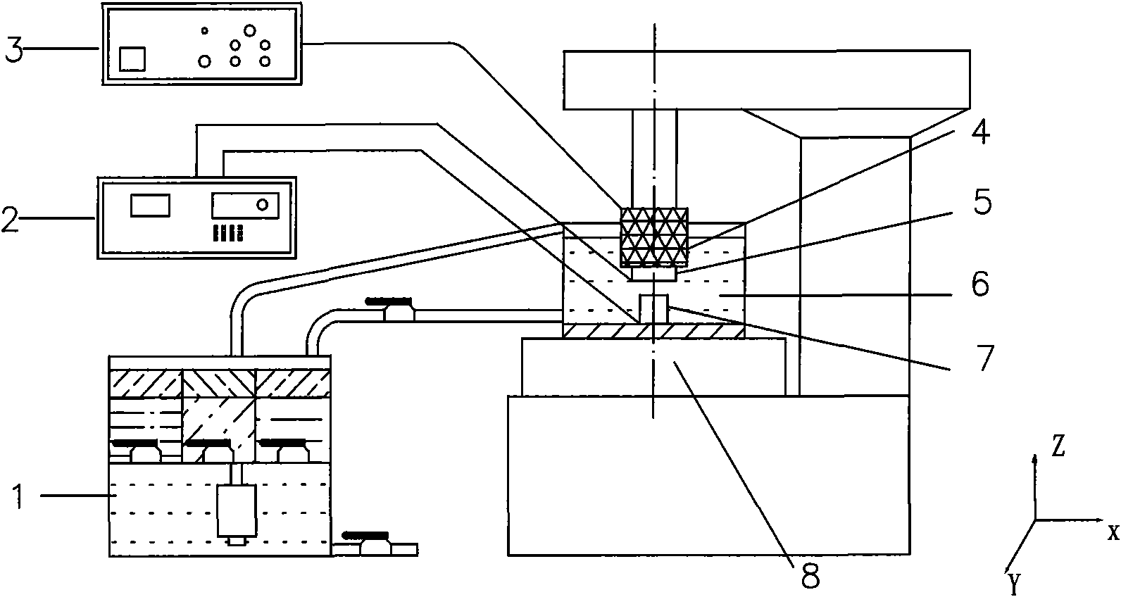
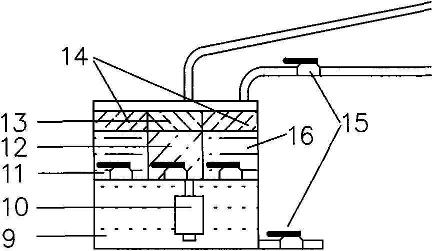
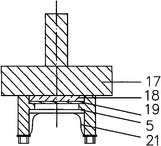
[0027] In the micro-EDM process, the micro-energy pulse power supply 2 strictly controls the single-pulse discharge energy (<50μJ) and its inter-electrode distribution to ensure sub-micron discharge gaps and realize semiconductor materials (resistivity <100Ω cm). Micro-etching and micro-electrodes are less and loss-free, and the positioning accuracy and feed resolution of the micro-electrodes are guaranteed through the three-coordinate sub-micron motion control platform 8, and semiconductor through holes are processed.

[0028]In order to improve the product removal status in the process of semiconductor vertical through-hole processing, on the one hand, measures such as the sub-micron working feed rate and rapid retraction of the inverted semiconductor workpiece 5 and the tool electrode 7 are adopted to reduce the phenomenon of short-circuit and arcing; on the other hand, By addin...


PUM

PropertyMeasurementUnit
electrical resistivityaaaaaaaaaa

Abstract

The invention discloses a method and a device for forming a vertical through hole in a semiconductor, which belong to the field of special machining. Based on a micro electromachining theory, the method uses a micro electrode array as a tool electrode and a semiconductor material (usually silicon, germanium, gallium arsenide, sapphire, silicon carbide and the like in sheet with a resistivity of less than 10 omega.cm) as a workpiece to process the vertical through hole(with a diameter phi of less than 50 mum and a depth to width ratio of less than 10) in the semiconductor by the processes of micro spark discharge, micro electrochemical finishing and side wall passivation sequentially. The device for implementing the method is provided with a device capable of continuously completing the processes of the micro spark discharge, the micro electrochemical finishing and the side wall passivation on one set of equipment for ensuring process integrity and positioning accuracy and is additionally provided with a shock wave generator capable of producing a shock wave effect for facilitating the machining of the through hole with a large depth to width ratio in the semiconductor. The technical method and the device have the characteristics of no relation with material crystal direction, vertical side wall, small heat affected zone, high machining precision, excellent technical flexibility and the like.

Description

technical field [0001] The present invention relates to the technical field of semiconductor micromachining, in particular to a method and device for forming vertical through-holes in semiconductors processed by microelectromachining technology. Vertical through hole processing. Background technique [0002] With the rapid development of modern information technology in the direction of high performance, low cost, and intelligence, semiconductor materials have become a leading technology in cutting-edge science and technology because of their unique electrical properties that are sensitive to changes in external factors such as light, heat, electricity, and magnetism. The most active application of advanced materials, especially in 3D IC packaging, MEMS packaging, vertical structure LED and vertically integrated sensor array (VISA) and other research and development needs is very urgent. The invention of Through-Silicon-Via (TSV, Through-Silicon-Via) technology has become o...

Claims


Application Information

Patent Timeline
Patent Type & Authority Applications(China)
IPC IPC(8): H01L21/302H01L21/60H01L21/768H01L21/00
Inventor 汪炜刘正埙丁维育田宗军刘志东沈理达黄因慧
Owner NANJING UNIV OF AERONAUTICS & ASTRONAUTICS
Why Eureka
Try Eureka