Storage unit of resistance storage and manufacture method thereof

A technology of resistive memory and storage unit, applied in static memory, read-only memory, digital memory information, etc., can solve problems such as the influence of RRAM reliability, and achieve the effect of improving resistance conversion performance and reducing oxygen content

Active Publication Date: 2009-11-11
SEMICONDUCTOR MANUFACTURING INTERNATIONAL (BEIJING) CORP
View PDF1 Cites 7 Cited by
  • Summary
  • Abstract
  • Description
  • Claims
  • Application Information

AI Technical Summary

Problems solved by technology

[0005] In addition, the storage medium 130 is formed by using plasma treatment (plasmatreatment) or thermal annealing (thermal annealing) process in an oxygen environment, usually an insulating metal oxide layer without binary resistance characteristics is formed on the surface of the dielectric film, for example figure 1 The shown dielectric film 131 and insulating metal oxide layer 132, and the insulating metal oxide layer 132 will affect the storage performance of the storage medium 130, taking metal oxide Cu as an example, the dielectric film 131 is low-priced cuprous oxide (Cu 2 O), the insulating metal oxide layer 132 is high-priced copper oxide (CuO), Cu 2 O has a binary resistance characteristic, while CuO does not have a binary resistance characteristic. Therefore, before writing data (programming) to the memory cell, it is necessary to apply a relatively large voltage to break down the insulating metal oxide layer 132. This will have a negative impact on the reliability of the RRAM

Method used


Image

  • Storage unit of resistance storage and manufacture method thereof
  • Storage unit of resistance storage and manufacture method thereof
  • Storage unit of resistance storage and manufacture method thereof

Examples


Embodiment 1

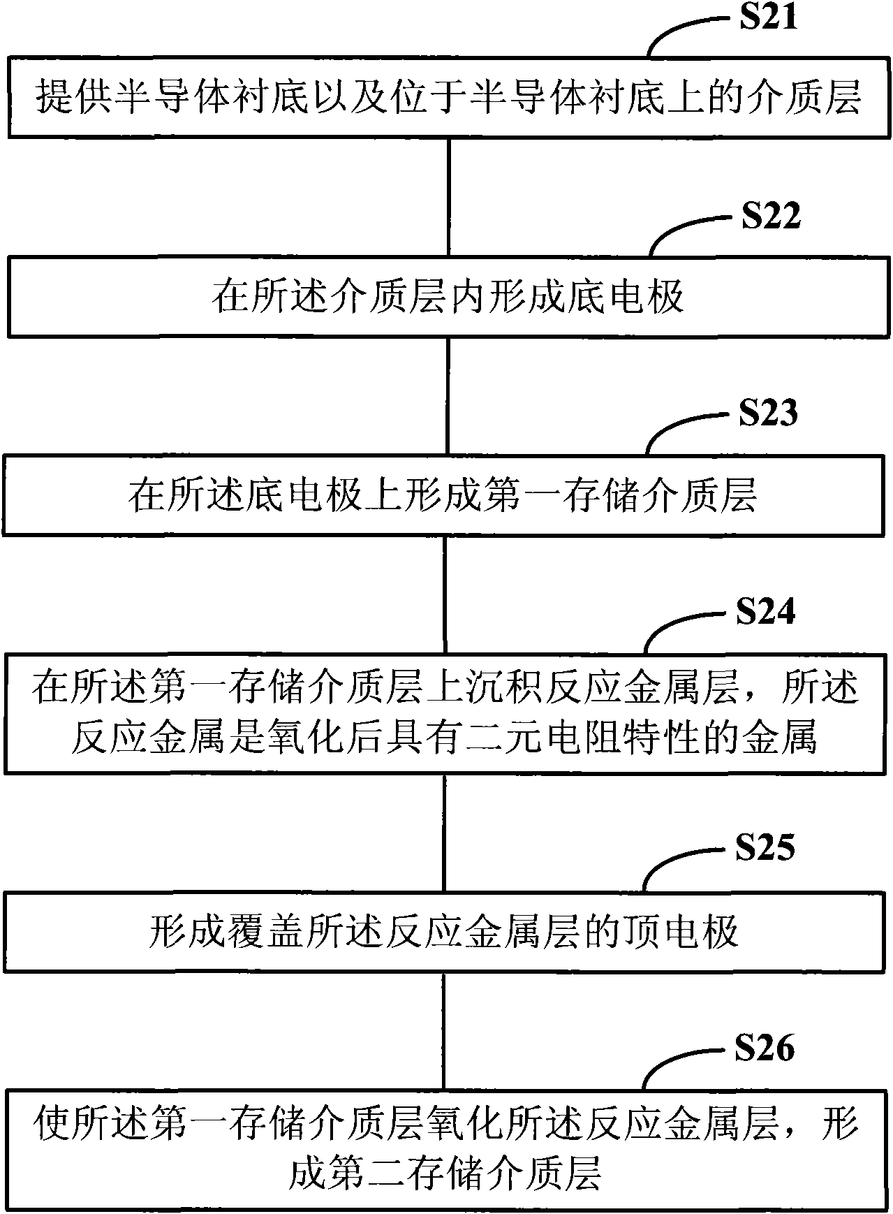
[0031] Please refer to the attached figure 2 , the manufacturing method of the storage unit of the resistive memory of the present embodiment, comprising:

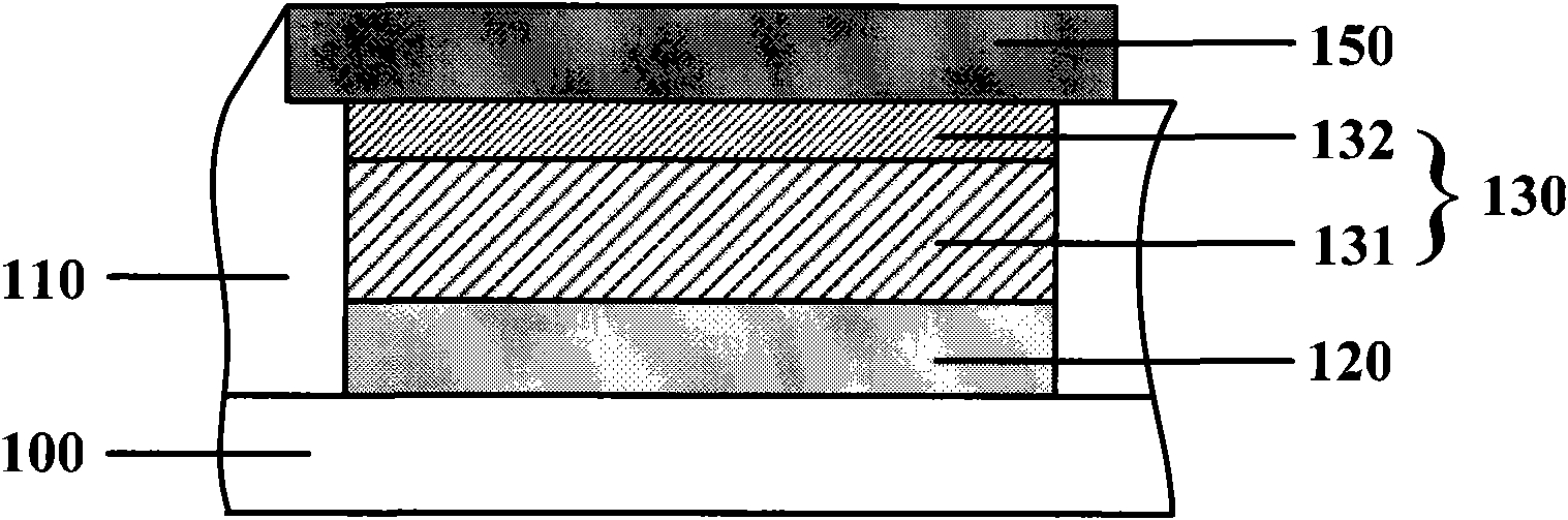
[0032] Step S21, providing a semiconductor substrate and a dielectric layer on the semiconductor substrate;

[0033] Step S22, forming a bottom electrode in the dielectric layer;

[0034] Step S23, forming a first storage medium layer on the bottom electrode;

[0035] Step S24, depositing a reactive metal layer on the first storage medium layer, the reactive metal is a metal having binary resistance characteristics after oxidation;

[0036] Step S25, forming a top electrode covering the reactive metal layer;

[0037] Step S26, oxidizing the reactive metal layer on the first storage medium layer to form a second storage medium layer.

[0038] Please refer to the attached figure 2 and 4, step S21 , providing a semiconductor substrate 200 and a dielectric layer 210 on the semiconductor substrate 200 . The semiconduct...

Embodiment 2

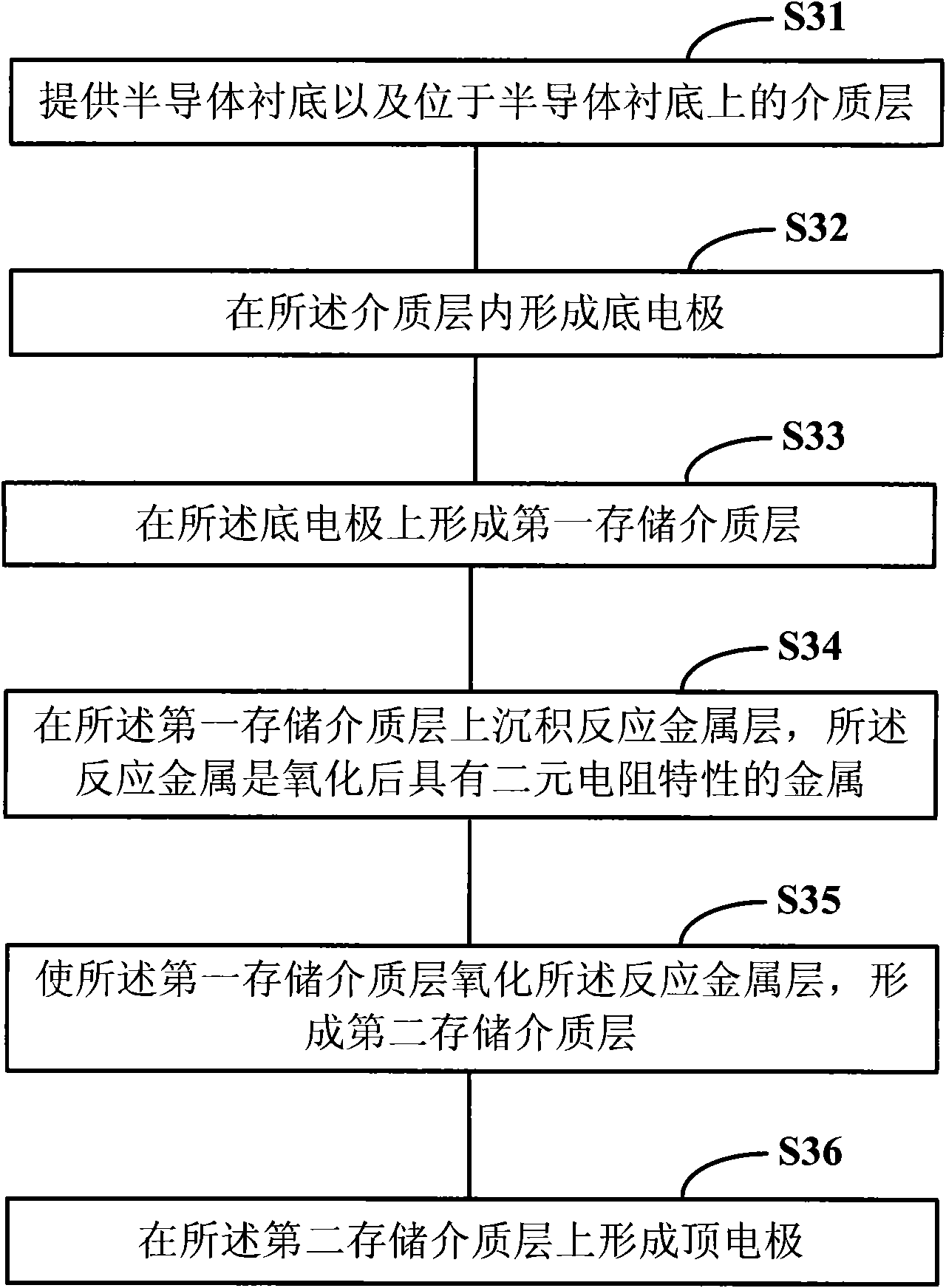
[0055] Please refer to the attached image 3 , the manufacturing method of the storage unit of the resistive memory of the present embodiment, comprising:

[0056] Step S31, providing a semiconductor substrate and a dielectric layer on the semiconductor substrate;

[0057] Step S32, forming a bottom electrode in the dielectric layer;

[0058] Step S33, forming a first storage medium layer on the bottom electrode;

[0059] Step S34, depositing a reactive metal layer on the first storage medium layer, the reactive metal is a metal having binary resistance characteristics after oxidation;

[0060] Step S35, making the first storage medium layer oxidize the reactive metal layer to form a second storage medium layer;

[0061] Step S36, forming a top electrode on the second storage medium layer.

[0062] The difference between this embodiment and Embodiment 1 is that in Embodiment 1, a top electrode is first formed on the reactive metal layer, and then the reactive metal layer i...


PUM

PropertyMeasurementUnit
thicknessaaaaaaaaaa
thicknessaaaaaaaaaa

Abstract

The invention discloses a storage unit of a resistance storage and a manufacture method thereof. The manufacture method of the storage unit comprises the following steps: providing a semiconductor substrate and a dielectric layer on the semiconductor substrate; forming a bottom electrode in the dielectric layer; forming a first storage dielectric layer on the bottom electrode; depositing a reaction metal layer on the first storage dielectric layer, wherein the reaction metal is metal having the characteristic of binary resistor after being oxidized; forming a top electrode covering the reaction metal layer; and enabling the first storage dielectric layer to oxidize the reaction metal layer to form a second storage dielectric layer. The storage unit of a resistance storage and the manufacture method thereof can reduce, control and regulate oxygen content in a first storage medium and enhance resistance conversion performance of the storage medium.

Description

technical field [0001] The invention relates to the technical field of semiconductor manufacturing, in particular to a storage unit of a resistance memory and a manufacturing method thereof. Background technique [0002] At present, the development of new storage technologies with low cost, high speed, high storage density, simple manufacturing and good compatibility with the current complementary metal oxide (CMOS) semiconductor integrated circuit process has attracted widespread attention worldwide. The memory technology of resistive random access memory (RRAM, referred to as resistive memory) based on metal oxides with resistive switching characteristics is currently the focus of development by many device manufacturers, because this technology can provide higher density, lower cost and lower power consumption non-volatile memory. The resistance value of the RRAM memory cell will change greatly after the pulse voltage is applied, and this resistance value can still be ma...

Claims


Application Information

Patent Timeline
Patent Type & Authority Applications(China)
IPC IPC(8): H01L45/00H01L27/24G11C11/56G11C16/02
Inventor 鲍震雷
Owner SEMICONDUCTOR MANUFACTURING INTERNATIONAL (BEIJING) CORP
Why Eureka
Try Eureka