

Multi-quantum-well structure used in photoelectron device and manufacturing method thereof
A multi-quantum well structure, optoelectronic device technology, applied in semiconductor/solid-state device manufacturing, electrical components, semiconductor devices, etc., can solve problems such as high production costs, numerous structures, and complex processes, achieving easy implementation and strong controllability , the effect of simple process
- Summary
- Abstract
- Description
- Claims
- Application Information
AI Technical Summary
Problems solved by technology
Method used
Image

Examples
Embodiment 1
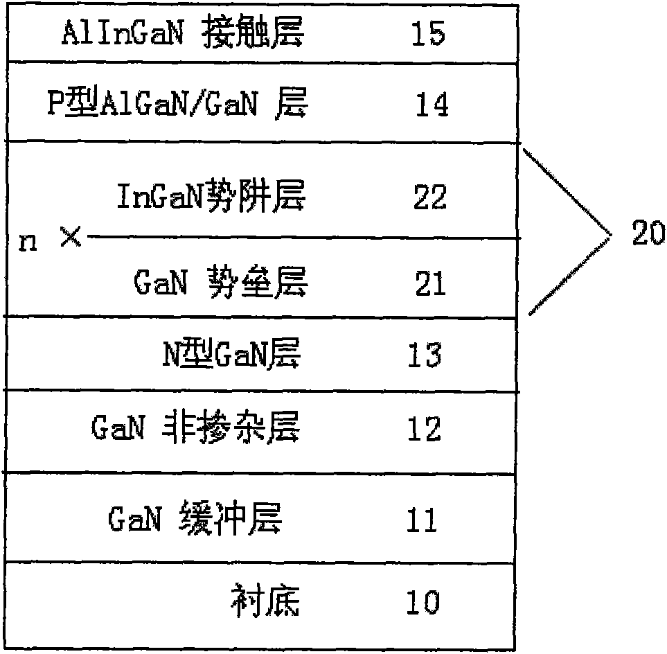
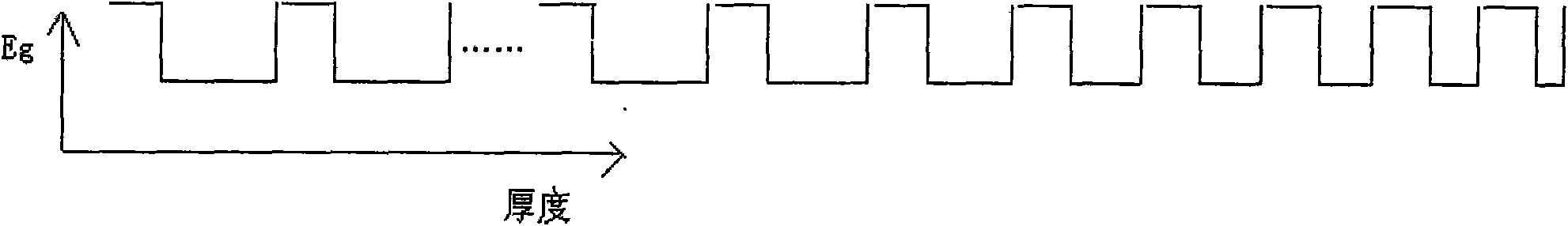
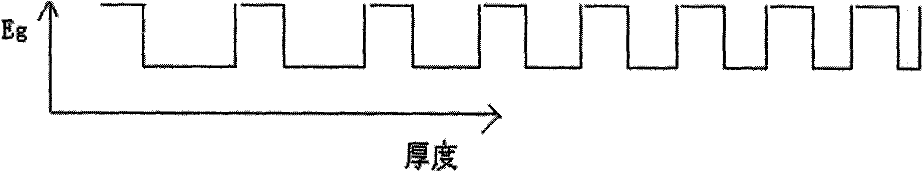
[0031] refer to figure 1 , the present embodiment provides a multi-quantum well structure 20 for optoelectronic devices, including n sequentially overlapping quantum well structures, the quantum well structure is formed by overlapping a potential barrier layer 21 and a potential well layer 22 in sequence, That is, it includes n barrier layers 21 and n potential well layers 22, the bandgap of the potential well layers 22 is smaller than that of the barrier layers 21, wherein n can be any integer greater than 2 and less than 20, and the optoelectronic device includes an N-type semiconductor Layer 13 and P-type semiconductor layer 14.
[0032] The barrier layer 21 can be a binary, ternary, or quaternary compound or mixture composed of Ga, In, Al, and N, including GaN, In x Ga 1-x N. Al y Ga 1-y N, In a Ga b Al 1-a-b N, where 0<x<1, 0<y<=1, 0<a<1, 0<b<1, and a+b<=1, is preferably GaN.
[0033] The potential well layer 22 can be a binary, ternary, or quaternary compound or ...
Embodiment 2
[0045] refer to figure 1 , the present embodiment provides a multi-quantum well structure 20 for optoelectronic devices, including n sequentially overlapping quantum well structures, the quantum well structure is formed by overlapping a potential barrier layer 21 and a potential well layer 22 in sequence, That is, it includes n barrier layers 21 and n potential well layers 22, the bandgap of the potential well layers 22 is smaller than that of the barrier layers 21, wherein n can be any integer greater than 2 and less than 20, and the optoelectronic device includes an N-type semiconductor Layer 13 and P-type semiconductor layer 14.
[0046] The barrier layer 21 can be a binary, ternary, or quaternary compound or mixture composed of Ga, In, Al, and N, including GaN, In x Ga 1-x N. Al y Ga 1-y N, In a Ga b Al 1-a-b N, where 0<x<1, 0<y<=1, 0<a<1, 0<b<1, and a+b<=1, is preferably GaN.
[0047] The potential well layer 22 can be a binary, ternary, or quaternary compound or ...
Embodiment 3
[0059] refer to figure 1 , the present embodiment provides a multi-quantum well structure 20 for optoelectronic devices, including n sequentially overlapping quantum well structures, the quantum well structure is formed by overlapping a potential barrier layer 21 and a potential well layer 22 in sequence, That is, it includes n barrier layers 21 and n potential well layers 22, the bandgap of the potential well layers 22 is smaller than that of the barrier layers 21, wherein n can be any integer greater than 2 and less than 20, and the optoelectronic device includes an N-type semiconductor Layer 13 and P-type semiconductor layer 14.
[0060] The barrier layer 21 can be a binary, ternary, or quaternary compound or mixture composed of Ga, In, Al, and N, including GaN, In x Ga 1-x N. Al y Ga 1-y N, In a Ga b Al 1-a-b N, where 0<x<1, 0<y<=1, 0<a<1, 0<b<1, and a+b<=1, is preferably GaN.
[0061] The potential well layer 22 can be a binary, ternary, or quaternary compound or ...
PUM
| Property | Measurement | Unit |
|---|---|---|
| Wavelength | aaaaa | aaaaa |
Abstract
Description
Claims
Application Information