Semiconductor processing device and nozzle structure used in same

A processing device and semiconductor technology, applied in the direction of semiconductor/solid-state device manufacturing, spraying device, spraying device, etc., can solve the problems of increased design difficulty, increased design difficulty, small space, etc., achieve flexible design and optimization, and improve cutting Erosion uniformity, the effect of improving the excellent rate

Active Publication Date: 2013-03-27
BEIJING NAURA MICROELECTRONICS EQUIP CO LTD
View PDF0 Cites 0 Cited by
  • Summary
  • Abstract
  • Description
  • Claims
  • Application Information

AI Technical Summary

Problems solved by technology

But the defect of this kind of scheme is that this kind of design can increase the difficulty of design, because there are many other parts above the chamber, such as plasma source etc. (such as figure 2 shown), so the space is small, and the interferometric device needs to be irradiated to the surface of a transparent object (not shown in the figure), and then projected into the chamber, so the original quartz window 103 needs to be redesigned, Add transparent parts and avoid intense plasma bombardment
Therefore, the design difficulty increases and the cost is higher
[0008] And on the other hand, the existing nozzle structure that injects gas from one end and ejects gas from the center of the tubular structure at the other end is also difficult to achieve the purpose of uniformly or radially injecting gas into the environment

Method used


Image

  • Semiconductor processing device and nozzle structure used in same
  • Semiconductor processing device and nozzle structure used in same
  • Semiconductor processing device and nozzle structure used in same

Examples


Embodiment Construction

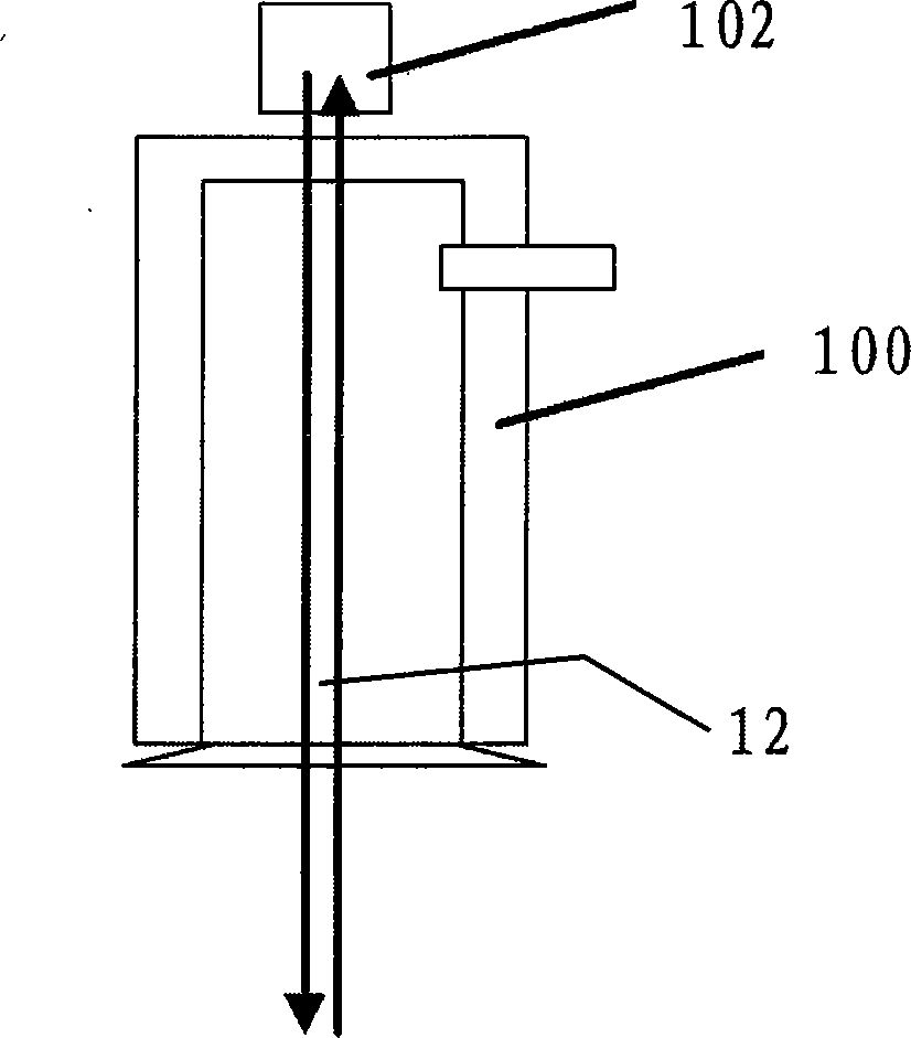
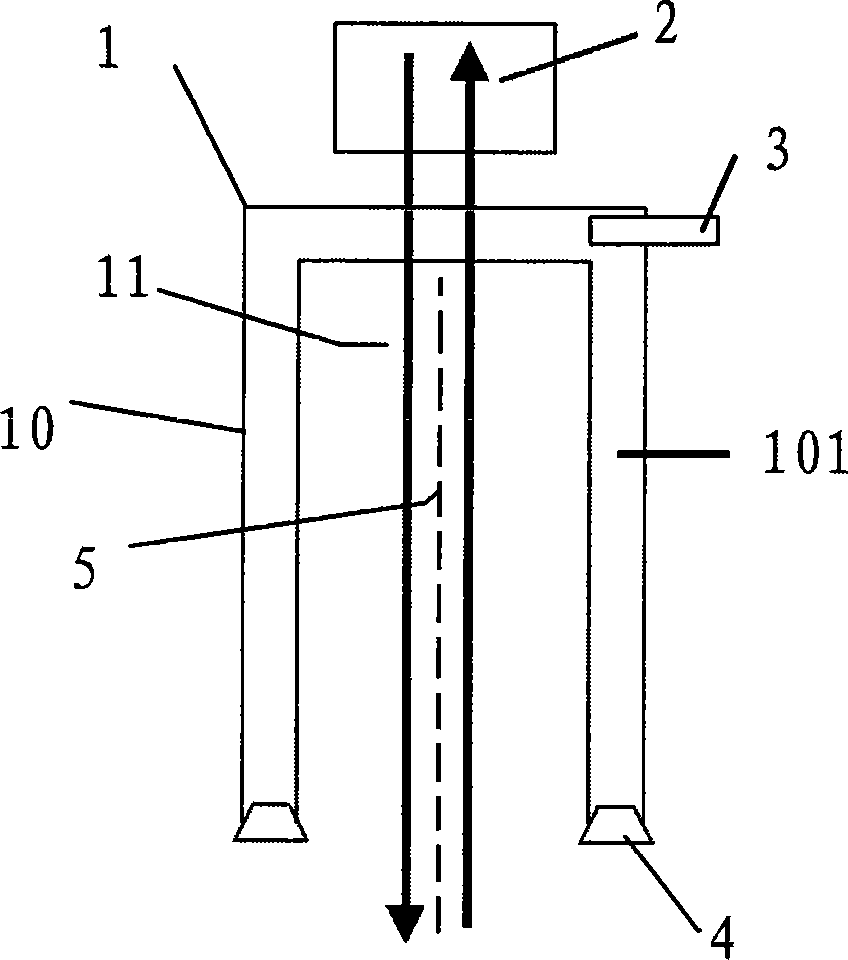
[0021] see image 3 , which shows a partial schematic diagram of a preferred embodiment of the present invention for a semiconductor processing device, which is provided with a nozzle (such as image 3 shown), for example, the nozzle is provided above the wafer in the etching equipment, image 3 Other structures of the semiconductor processing device are not shown in the figure, but these structures are well known or obvious to those skilled in the art. The nozzle includes a columnar body 1 with an inner diameter. Generally, the exterior of the body is also columnar, including cylinders or cylinders with polygonal cross-sections. The body 1 is also provided with a gas inlet 3 and a gas outlet 4 . Moreover, the gas inlet 3 is located on the upper edge of the body 1, the gas outlet 4 is located at the bottom of the side wall 10 of the body 1, and a Air flow channel 101, the air flow channel 101 communicates with the gas inlet 3 and the gas outlet 4, the air flow channel 101 of...


PUM


Abstract

The invention relates to a semiconductor processing device and a corresponding nozzle structure, wherein a nozzle comprises a body of which an inner path is columnar; a gas inlet and a gas outlet are arranged on the body; the gas inlet is positioned on the edge of the upper part of the main body; the gas outlet is positioned on the bottom of the sidewall of the body; a gas flow channel is formed in the sidewall of the body or on the inner side of the sidewall; the gas flow channel is communicated with the gas inlet and the gas outlet; and the exit direction of the gas outlet is at an angle between 0 and 85 degrees to a center vertical line of the body. The invention can separate gas jetted downwards from the nozzle and a downward-irradiating optical path of an interference measurement device from each other, avoids bombardment to the nozzle because a place just below the nozzle is high in plasma density, then prevents the design of a gas nozzle from interfering in application effects of the interference measurement device, and provides more flexible space for the design and optimization of the gas nozzle so as to ensure that the nozzle is simple in structure and obvious in effects.

Description

technical field [0001] The invention relates to a semiconductor processing device and a nozzle structure used in the semiconductor processing device. Background technique [0002] In the semiconductor processing industry, as the processing technology nodes become smaller and smaller, the requirements for the uniformity of the entire silicon wafer-scale processing process are getting higher and higher. Generally, it can be done by modifying the setting parameters of the process, or by modifying the hardware Symmetry modifications improve uniformity. Appropriately modifying the design of these hardware is of great help to improve the uniformity of the etching process. However, due to the application of integrated measurement equipment, such as interferometric equipment, sometimes the modification of the hardware is restricted or conflicts with the modification of the hardware. [0003] Moreover, most of the existing nozzle structures are air intake from one end, and the gas ...

Claims


Application Information

Patent Timeline
Patent Type & Authority Patents(China)
IPC IPC(8): B05B1/14H01L21/02
Inventor 陈卓
Owner BEIJING NAURA MICROELECTRONICS EQUIP CO LTD
Why Eureka
Try Eureka