Thin film transistor, manufacturing method thereof, array substrate, and display device

a manufacturing method and thin film transistor technology, applied in the field can solve the problems of deterioration stability, affecting stability and other properties of thin film transistors, and unstable thin film transistors, so as to and improve the stability of ltps thin film transistors. stability and other problems, to achieve the effect of improving the stability of array substrates

Active Publication Date: 2017-02-09
BOE TECH GRP CO LTD
View PDF1 Cites 0 Cited by
  • Summary
  • Abstract
  • Description
  • Claims
  • Application Information

AI Technical Summary

Benefits of technology

[0005]In view of the above drawbacks existing in the prior art, the technical problem to be solved by the present invention is to provide a manufacturing method of a thin film transistor, a thin film transistor, an array substrate and a display device. By using the manufacturing method of a thin film transistor, defect states and unstable factors of interface in the thin film transistor can be reduced, thereby improving stability of the LTPS thin film transistor and achieving more stable performance of the array substrate and the display device.
[0025]In the manufacturing method of a thin film transistor, bombardment and damage to the surface of poly-silicon P-Si during channel doping is avoided mainly by optimizing crystallization and doping process of the active layer, thereby reducing defect states and dangling bonds at the surface of poly-silicon P-Si caused by bombardment. Meanwhile dopant ions are concentrated in a relatively narrow region close to the interface by forming poly-silicon layers P-Si separately, and compared with a thin film transistor device in which dopant ions are widely distributed, distributions of deep traps and charged impurities are reduced, and thereby unstable factors near the interface such as defect states, dangling bonds, movable ions and the like are reduced. It can be seen that, the manufacturing method of a thin film transistor can improve and optimize properties and other aspect of a LTPS (Low Temperature Poly-Silicon) thin film transistor, as a result, defect states and other unstable factors in the thin film transistor are reduced, stability of the thin film transistor is improved and overall performance of the thin film transistor is improved as well.
[0026]The array substrate can achieve more stable performance because it adopts thin film transistors having relatively high stability.
[0027]The display device can achieve more stable performance because it adopts thin film transistors having relatively high stability and the corresponding array substrate.

Problems solved by technology

In the process of adding dopant ions by ion implantation, the interface of the poly-silicon is inevitably damaged by high-energy ions, and can only be repaired incompletely even after subsequent high-temperature annealing, which deteriorates stability of the thin film transistor; meanwhile, the energy of ion implantation itself has a certain distribution, in the subsequent activation process, the doped ions can hardly be distributed evenly and bonded tightly with the neighboring atoms, which makes the thin film transistor even more unstable under the impact of external energy such as heat, light and electricity.
Since the interface and crystalline portion of poly-silicon may be damaged and have a relatively low stability, the stability and other properties of the thin film transistor are impacted.

Method used


Image

  • Thin film transistor, manufacturing method thereof, array substrate, and display device
  • Thin film transistor, manufacturing method thereof, array substrate, and display device
  • Thin film transistor, manufacturing method thereof, array substrate, and display device

Examples


embodiment 1

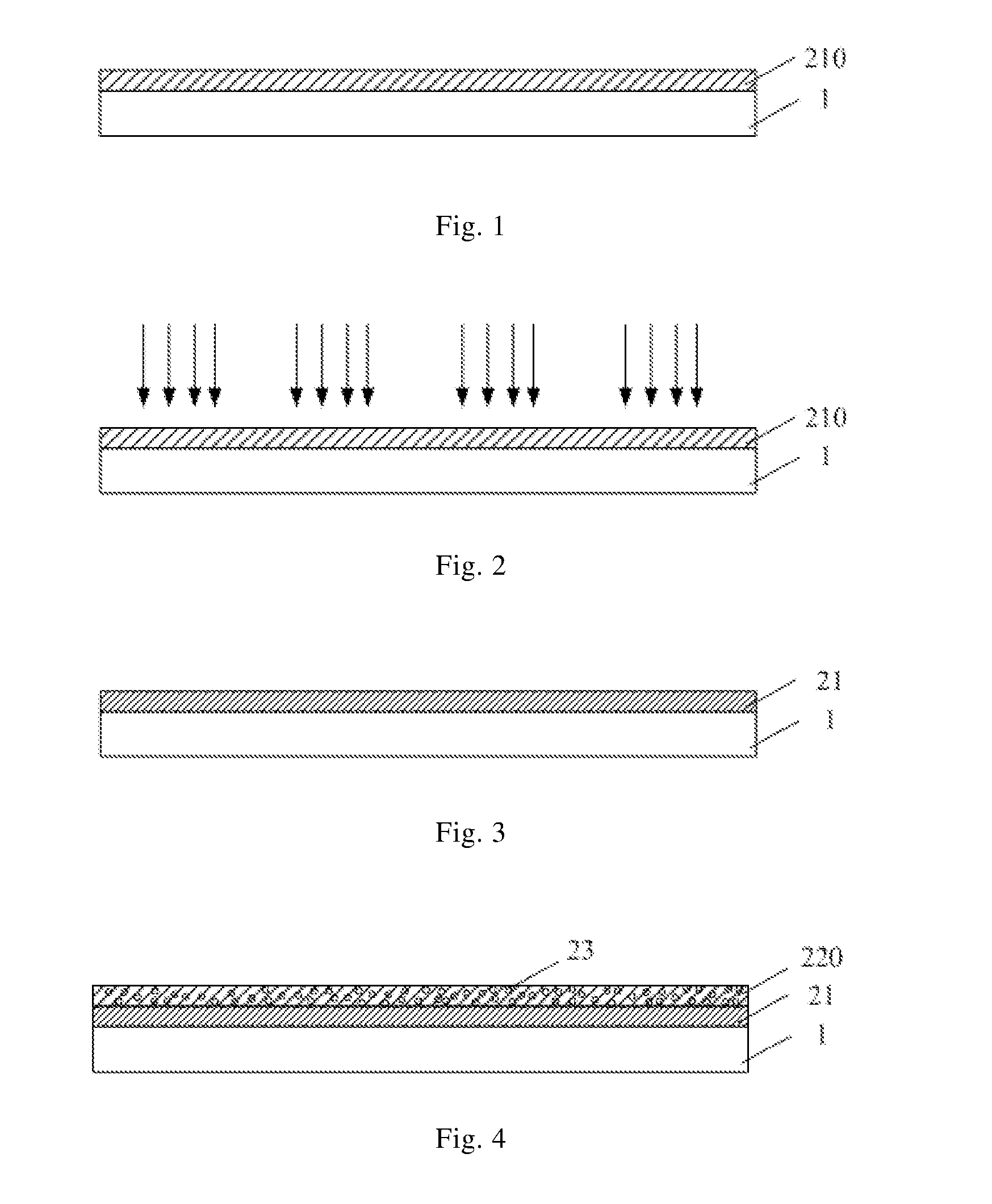
[0035]The embodiment provides a manufacturing method of a thin film transistor and a thin film transistor manufactured by using the manufacturing method. By using the manufacturing method of a thin film transistor, defect states and other unstable factors of the interface in the thin film transistor can be reduced, and the thin film transistor formed by using the manufacturing method of a thin film transistor has relatively high stability and relatively good performance.

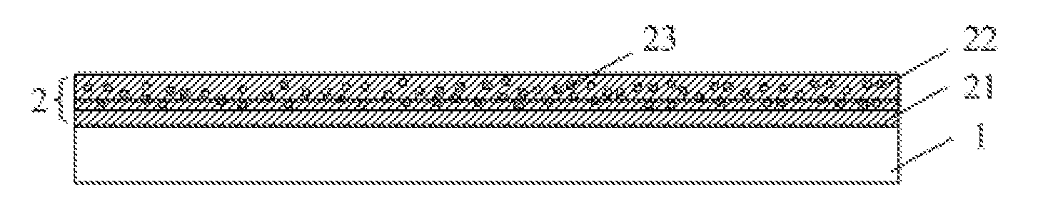
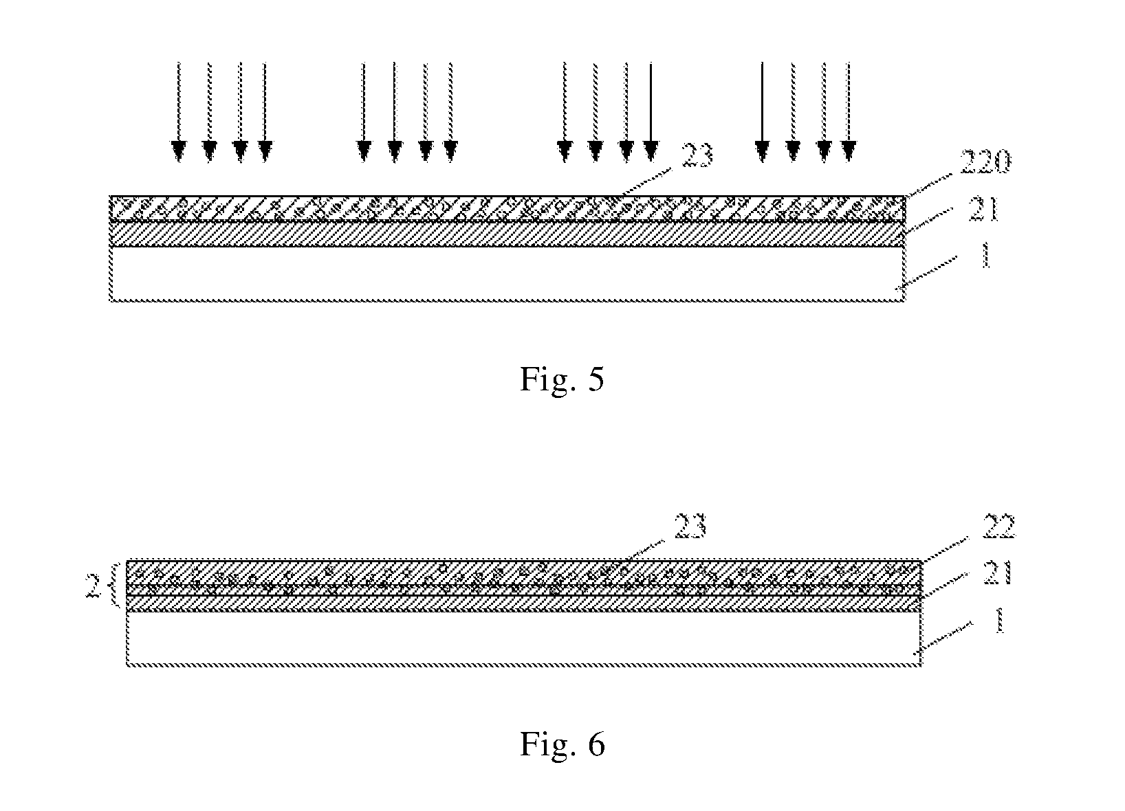
[0036]The manufacturing method of a thin film transistor provided by the embodiment includes a step of forming an active layer, and the step of forming an active layer includes: forming a first poly-silicon layer and a second poly-silicon layer on the first poly-silicon layer separately, and doping dopant ions into the second poly-silicon layer and an upper surface layer of the first poly-silicon layer.

[0037]Thereinafter, the manufacturing method of a thin film transistor is described in detail with reference to the ...

embodiment 2

[0061]This embodiment provides an array substrate comprising the thin film transistor in Embodiment 1, and the array substrate is applicable to liquid crystal display devices and OLED display devices.

[0062]The array substrate in the embodiment may include other layer structures such as a passivation layer, a pixel electrode layer (for a liquid crystal display device) or a pixel define layer (for an OLED display device), and the like. The specific structures and manufacturing process of these layer structures may refer to those in the prior art, and are not repeatedly described herein.

[0063]The array substrate can achieve more stable performance because it adopts thin film transistors having relatively high stability.

embodiment 3

[0064]This embodiment provides a display device comprising the array substrate in Embodiment 2.

[0065]The display device may be any product or component having a display function, such as a liquid crystal panel, electronic paper, an OLED panel, a mobile phone, a tablet computer, a television, a display, a notebook computer, a digital photo frame, a navigator, or the like.

[0066]The display device can achieve more stable performance because it adopts thin film transistors having relatively high stability and the corresponding array substrate.


PUM

PropertyMeasurementUnit
thicknessaaaaaaaaaa
thicknessaaaaaaaaaa
thicknessaaaaaaaaaa

Abstract

Embodiments of the present invention disclose a manufacturing method of a thin film transistor, a thin film transistor, an array substrate and a display device. The manufacturing method of a thin film transistor includes a step of forming an active layer, and the step of forming an active layer includes: forming a first poly-silicon layer and a second poly-silicon layer on the first poly-silicon layer separately, and adding dopant ions into the second poly-silicon layer and an upper surface layer of the first poly-silicon layer. By using the manufacturing method of a thin film transistor, defect states and unstable factors of interface in the thin film transistor can be reduced, thereby improving stability of the LTPS thin film transistor and obtaining an array substrate and a display device having more stable performance.

Description

FIELD OF THE INVENTION[0001]The present invention relates to the field of display technology, in particular to a thin film transistor, a manufacturing method thereof, an array substrate and a display device.BACKGROUND OF THE INVENTION[0002]Low Temperature Poly-Silicon (LTPS for short) thin film transistors have higher electron mobility compared with conventional amorphous silicon thin film transistors. The electron mobility of a LTPS thin film transistor can generally reach 50-200 cm2 / V-sec, and thus the area of channel can be effectively reduced, so that the area of the thin film transistor can be reduced. By applying the LTPS thin film transistors in a display device, the aperture ratio and integration of the display device can be improved, and as a result, the brightness of the display device can be improved while the power consumption thereof is reduced.[0003]LTPS is generally used for forming an active layer of a thin film transistor. At present, preparation process for an acti...

Claims


Application Information

Patent Timeline
Patent Type & Authority Applications(United States)
IPC IPC(8): H01L29/786H01L21/02H01L27/12H01L21/306H01L21/225H01L29/10H01L29/66H01L21/30
CPCH01L29/78675H01L29/66757H01L21/02532H01L21/02592H01L21/02675H01L27/1285H01L21/30604H01L21/2251H01L29/78696H01L29/1033H01L27/1222H01L21/3003H01L21/77H01L29/78672H01L27/127H01L29/786
Inventor TIAN, HONGWEINIU, YANANWANG, ZUQIANGSUN, LIANG
Owner BOE TECH GRP CO LTD
Why Eureka
Try Eureka