Manufacturing method of semiconductor laser vertical ridge structure capable of accurately controlling height

A technology of precise control and manufacturing method, applied to the structure of optical waveguide semiconductors, etc., can solve the problems of easy loose deformation, carbonization and shedding of photoresist, and failure, so as to improve the output efficiency of single-mode laser, reduce the current injection area, The effect of improving the verticality and smoothness of the side wall

Pending Publication Date: 2022-07-01
Shandong Huaguang Optoelectronics Co. Ltd.
View PDF1 Cites 0 Cited by
  • Summary
  • Abstract
  • Description
  • Claims
  • Application Information

AI Technical Summary

Problems solved by technology

However, photoresist on SiO 2 The structure under the mask, in the dry etching process, is subjected to high temperature and plasma, and the photoresist is easy to loosen, deform or even carbonize and fall off, resulting in the failure of the entire etching process.

Method used


Image

  • Manufacturing method of semiconductor laser vertical ridge structure capable of accurately controlling height
  • Manufacturing method of semiconductor laser vertical ridge structure capable of accurately controlling height
  • Manufacturing method of semiconductor laser vertical ridge structure capable of accurately controlling height

Examples


Embodiment 1

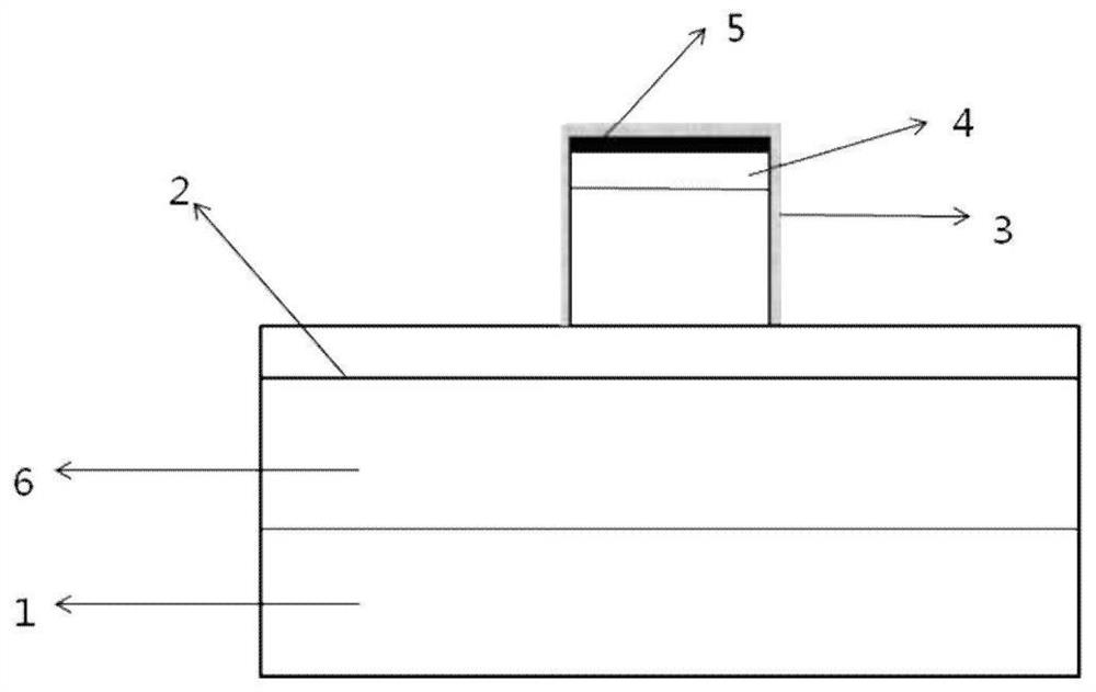
[0055] This embodiment provides a method for fabricating a vertical ridge structure of a semiconductor laser that can precisely control the height. The operation steps are as follows:

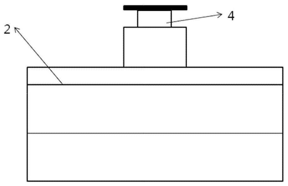
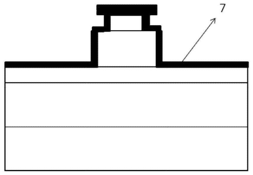
[0056] (1) The lower confinement layer, the lower waveguide layer, the active layer, the upper waveguide layer, the etching barrier layer 2, the upper confinement layer and the GaAs contact layer 4 are grown sequentially from bottom to top on the substrate 1. The etching barrier layer is selected according to the The material film layer that is difficult to corrode by hydrochloric acid solution according to the principle of natural corrosion;

[0057] (2) Deposition of SiO on the epitaxial wafer by PVD or PECVD 2 Do dry etching once mask 5, the thickness of one mask 5 is

[0058] (3) spin-coating photoresist 3 on the epitaxial wafer with the mask, the thickness of the photoresist is A periodic photoresist mask pattern adapted to the size of the ridge stripe is obtained by photolithography ...

Embodiment 2

[0071] A method for manufacturing a vertical ridge structure of a semiconductor laser that can precisely control the height, the operation steps are as described in Embodiment 1, the difference is that the thickness of the primary mask in step (2) is The thickness of the photoresist in step (3) is In step (5), the etching depth is greater than that of the etching barrier layer In step (8), the thickness of the secondary mask is SiO in step (12) 2 The thickness of the current blocking layer is Thickness of photoresist in step (13)

Embodiment 3

[0073] A method for manufacturing a vertical ridge structure of a semiconductor laser that can precisely control the height, the operation steps are as described in Embodiment 1, the difference is that in step (3), the size of the ridge stripe is 5 μm in width;

[0074] Step (7), GaAs special etching solution composition and mass ratio are H 3 PO 4 :H 2 O=2:3;

[0075] In step (8), the thickness of the secondary mask is

[0076] In step (10), hydrochloric acid solution components and mass ratio are HCl:H 2 O=1:5, the corrosion time is 10-200 seconds;

[0077] In step (11), silicon dioxide etching liquid component and mass ratio are HF:H 2 O=1:10.


PUM

PropertyMeasurementUnit
Widthaaaaaaaaaa

Abstract

The invention provides a manufacturing method of a vertical ridge structure of a semiconductor laser capable of accurately controlling the height. The manufacturing method comprises the following steps: growing a semiconductor epitaxial film layer and an ESL; sequentially forming a primary silicon dioxide mask and a primary photoresist mask on the epitaxial wafer, and photoetching to form a periodic ridge window; carrying out ICP etching on the silicon oxide mask; continuously performing ICP etching on the epitaxial layer to a certain depth to form a narrow ridge structure; removing the residual photoresist; corroding the GaAs contact layer to form an internal shrinkage structure; growing and carrying out ICP etching on a silicon dioxide mask for the second time; performing wet etching on the epitaxial film layer to the corrosion barrier layer; after the mask is removed, growing a SiO2 current blocking layer, and forming a secondary photoresist mask pattern; and ICP etching is carried out to remove the current blocking layer at the top of the GaAs, a current injection window is exposed, and manufacturing of the ridge-shaped structure is completed. A dry etching and wet etching combined mode is adopted, the ridge height can be accurately controlled, the side wall is vertical, meanwhile, a current injection area on a ridge strip is reduced, and the current injection density is improved.

Description

technical field [0001] The invention relates to a method for manufacturing a vertical ridge structure of a semiconductor laser that can precisely control the height, and belongs to the technical field of semiconductor lasers. Background technique [0002] Semiconductor lasers have the advantages of small size, light weight, and power saving, and are widely used in laser printing and printing, optical measurement, robotics and automatic control, beauty, medical and other fields. [0003] At present, the structure of the light-emitting region of semiconductor lasers is usually ridge-stripe. For lasers that require stable output of a single transverse mode spot, a narrow and rectangular ridge-shaped structure is very important. The commonly used method for fabricating the ridge structure is wet etching or dry etching. For the epitaxial structure of the multilayer film system, the isotropy and selectivity of wet etching can cause the ridges to be non-vertical, or it is easy to ...

Claims


Application Information

Patent Timeline
IPC IPC(8): H01S5/20H01S5/22
CPCH01S5/22H01S5/2206H01S5/2009
Inventor 任夫洋苏建郑兆河徐现刚
Owner Shandong Huaguang Optoelectronics Co. Ltd.
Why Eureka
Try Eureka