

Photomask, thin film transistor element and manufacturing method of thin film transistor element
A technology of thin-film transistors and photomasks, which is applied in the direction of transistors, semiconductor/solid-state device manufacturing, electrical components, etc., can solve the problems of decreased aperture ratio, difficulties, and increased resistance and capacitance loads, and achieve the effect of high turn-on current
- Summary
- Abstract
- Description
- Claims
- Application Information
AI Technical Summary
Problems solved by technology
Method used
Image

Examples
Embodiment Construction
[0027] In order for those skilled in the art to have a better understanding of the present invention, several preferred embodiments of the present invention are listed below, together with the accompanying drawings, to describe in detail the composition and desired effects of the present invention.
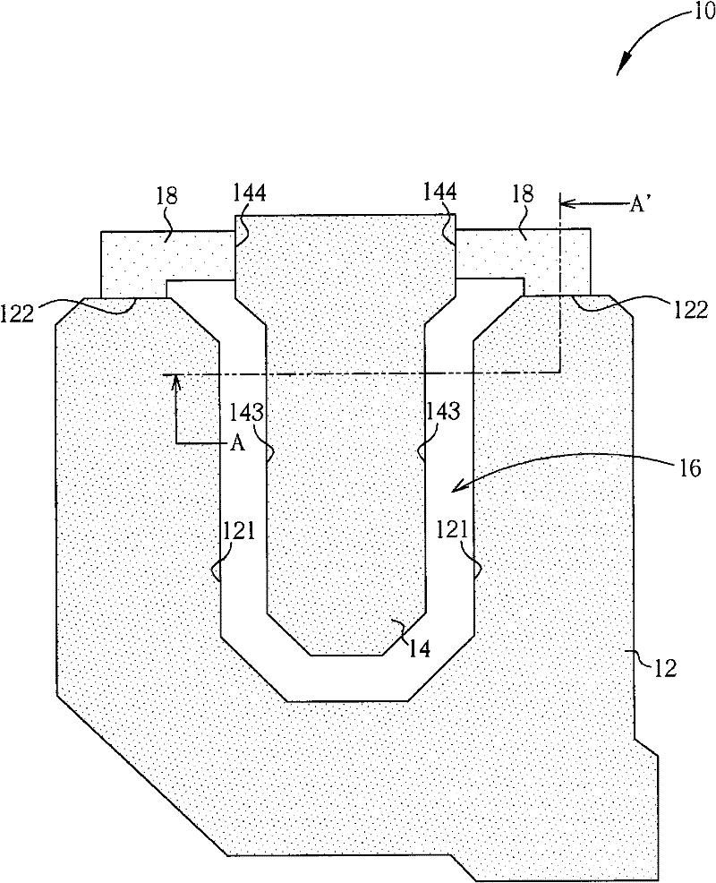
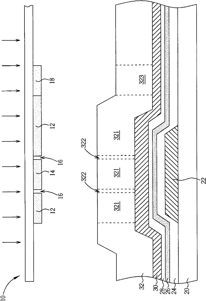
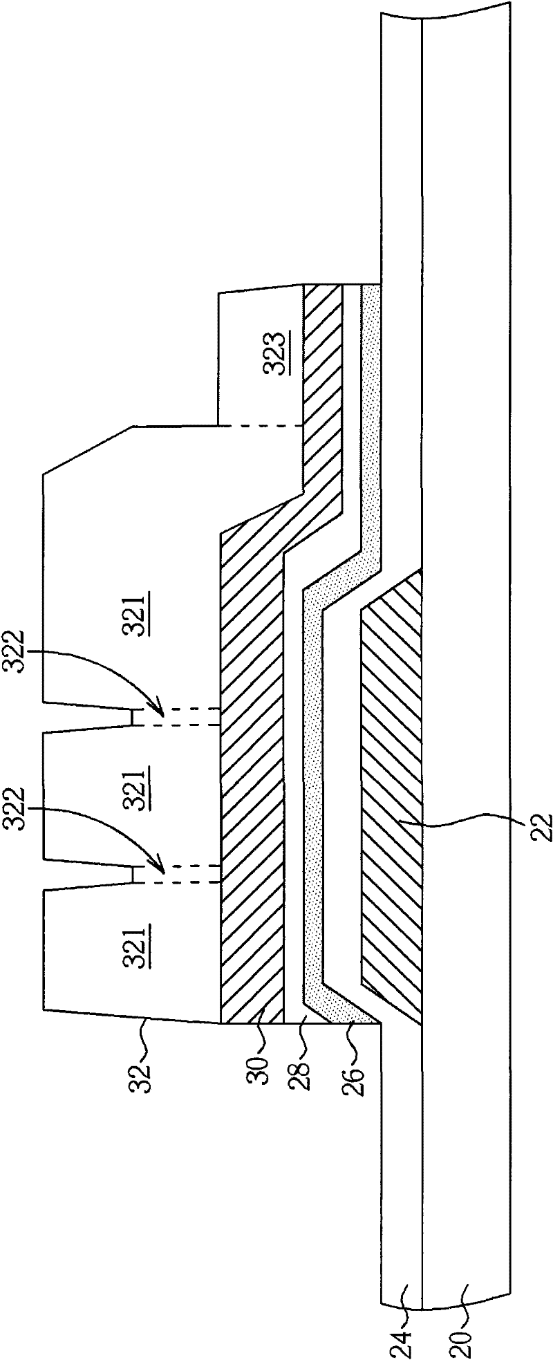
[0028] Please refer to figure 1 . figure 1 A schematic diagram of a photomask according to a preferred embodiment of the present invention is shown. In this embodiment, the photomask 10 may be a graytone mask (GTM), a halftone mask (HTM) or other photomasks that have different transmittances in different regions. . The photomask 10 of this embodiment includes a first light-shielding pattern 12 , a second light-shielding pattern 14 , a single light-transmitting slit 16 and a semi-transparent pattern 18 . The first light-shielding pattern 12 includes a first side 121 and a second side 122, the second light-shielding pattern 14 includes a third side 143 and a fourth side 144, and ...
PUM
| Property | Measurement | Unit |
|---|---|---|
| length | aaaaa | aaaaa |
| transmittivity | aaaaa | aaaaa |
| width | aaaaa | aaaaa |
Abstract
Description
Claims
Application Information