SRAM dual-position unit wiring method

A wiring method and bit cell technology, applied in electrical components, semiconductor/solid-state device manufacturing, circuits, etc., can solve the problems of increasing the coupling capacitance of surrounding wiring and increasing the resistance of its own wiring, so as to improve the working characteristics and reduce the Coupling capacitors, the effect of reducing resistance

Inactive Publication Date: 2009-12-09
GRACE SEMICON MFG CORP
View PDF3 Cites 11 Cited by
  • Summary
  • Abstract
  • Description
  • Claims
  • Application Information

AI Technical Summary

Problems solved by technology

[0007] The object of the present invention is to provide a kind of SRAM double-bit cell wiring method, to solve the existing method when BL and BLb use Metal3 to carry out wiring, increase the resistance on the self-connecting line and increase the problem of the coupling capacitance with peripheral wiring

Method used


Image

  • SRAM dual-position unit wiring method
  • SRAM dual-position unit wiring method
  • SRAM dual-position unit wiring method

Examples


Embodiment Construction

[0018] In order to make the purpose and features of the present invention more comprehensible, the specific implementation manners of the present invention will be further described below in conjunction with the accompanying drawings.

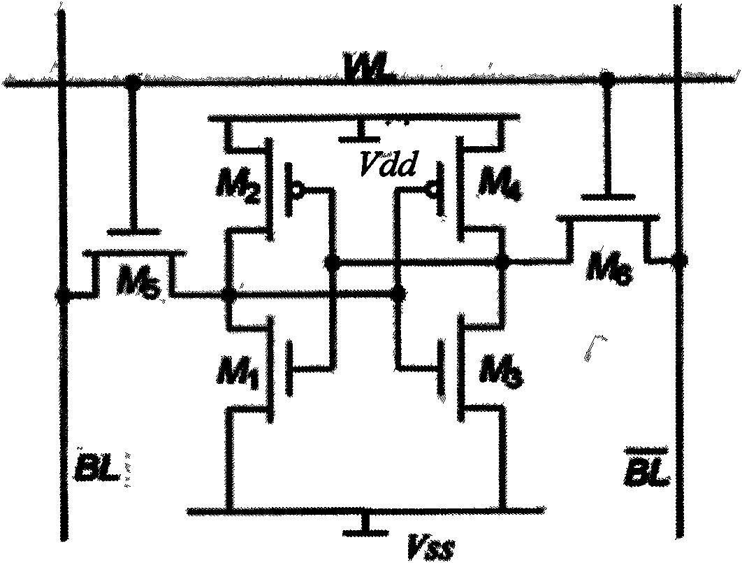
[0019] It has been mentioned in the background technology that in the layout of the existing 2x2SRAM cell, the bit lines BL and BLb use higher-level Metal3 for wiring, which not only increases the resistance on its own wiring, but also increases the connection with the surrounding wiring. Coupling capacitors reduce the operating characteristics of the SRAM.

[0020] The core idea of ​​the present invention is that the bit lines BL and BLb are wired using lower-level Metal2, and the word line WL is wired using Metal3, thereby greatly reducing the parasitic resistance and capacitance of the bit lines BL and BLb, and improving the performance of the SRAM. working characteristics.

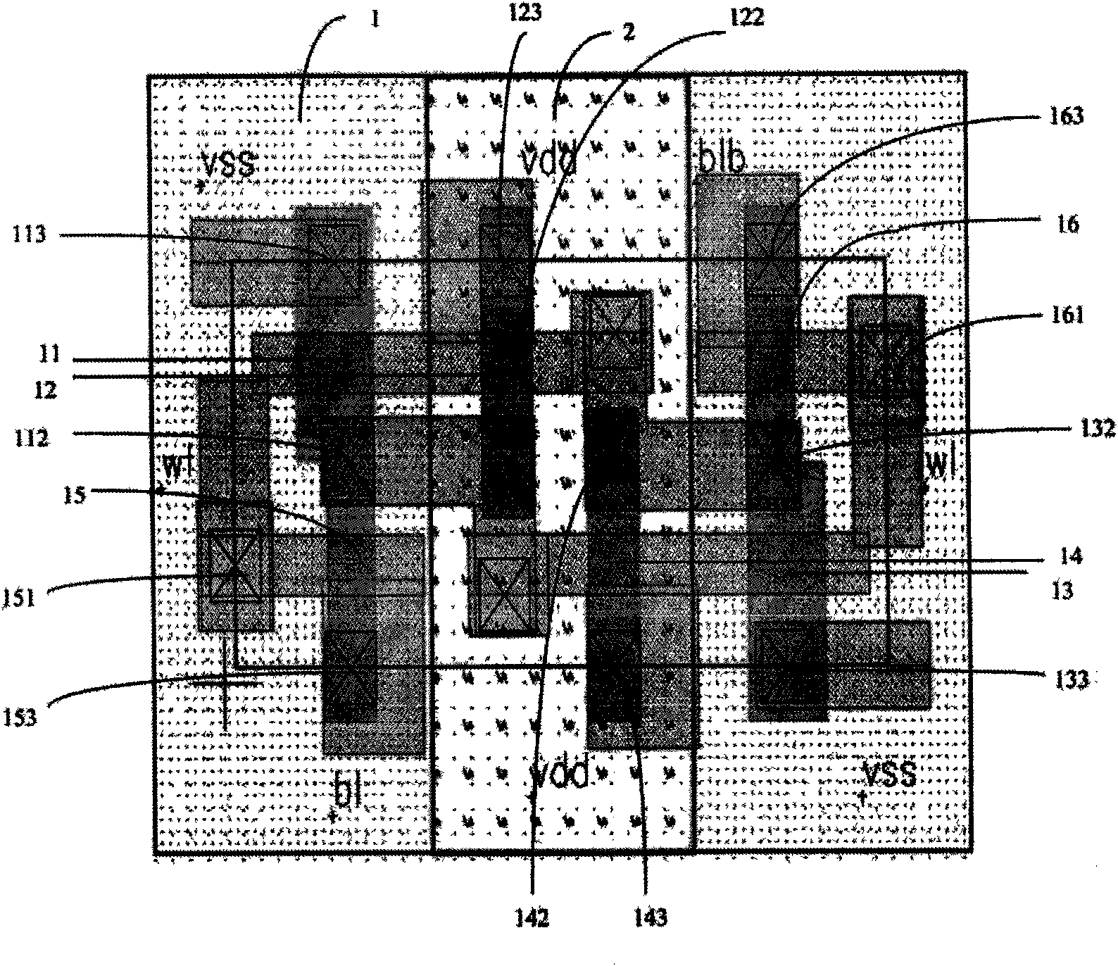
[0021] Figure 6 For the present invention in such as figure 2...


PUM


Abstract

The invention discloses an SRAM dual-position unit wiring method which wires bit lines BL and BLb, and power lines Vss and Vdd along vertical direction by Metal 2, and wires a word line WL along horizontal direction by Metal 3, which not only reduces resistance on connection lines of bit lines BL and BLb, but also reduces coupling capacitance of bit lines BL and BLb and circumferential wired lines, so that performance characteristic of SRAM is improved. In addition, the bit lines BL and BLb are wired by Metal 2 so that metal wiring above SRAM has one more selection.

Description

technical field [0001] The invention relates to a semiconductor device wiring method, in particular to a SRAM double-bit cell wiring method, and belongs to the technical field of silicon semiconductor devices. Background technique [0002] Static Random Access Memory (SRAM) is a type of semiconductor memory that retains data as long as power is supplied. SRAM has the advantages of low power consumption, fast data access speed and compatibility with CMOS logic technology, and is widely used in various electronic devices. [0003] A basic SRAM cell consists of two cross-coupled inverters and two access transistors. A typical six-transistor SRAM (6T SRAM) cell circuit structure is as follows figure 1 shown. Among them, the CMOS inverter composed of M1 and M2 is cross-coupled with the CMOS inverter composed of M3 and M4 to latch a binary number, and M5 and M6 are access transistors, which are stored when the memory is read and written. The function of connecting or disconnec...

Claims


Application Information

Patent Timeline
Patent Type & Authority Applications(China)
IPC IPC(8): H01L21/8244H01L21/768
Inventor 胡剑孔蔚然
Owner GRACE SEMICON MFG CORP
Why Eureka
Try Eureka