Method for graphene epitaxial growth on 4H-SiC silicon surface

A technology of epitaxial growth and graphene, applied in the field of microelectronics, which can solve the problems of difficult control of the growth process, low uniformity, and small area of ​​Graphene

Inactive Publication Date: 2011-04-27
XIDIAN UNIV
View PDF0 Cites 5 Cited by
  • Summary
  • Abstract
  • Description
  • Claims
  • Application Information

AI Technical Summary

Problems solved by technology

Disadvantages: the growth process is difficult to control, and it is difficult to obtain large-scale uniform samples
Using this epitaxial growth method, although Graphene with high quality and large size can be obtained, there are many factors that make the area of ​​the grown Graphene too small and the uniformity is not high.

Method used


Image

  • Method for graphene epitaxial growth on 4H-SiC silicon surface
  • Method for graphene epitaxial growth on 4H-SiC silicon surface
  • Method for graphene epitaxial growth on 4H-SiC silicon surface

Examples


Embodiment 1

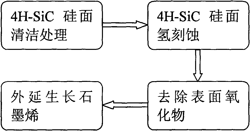
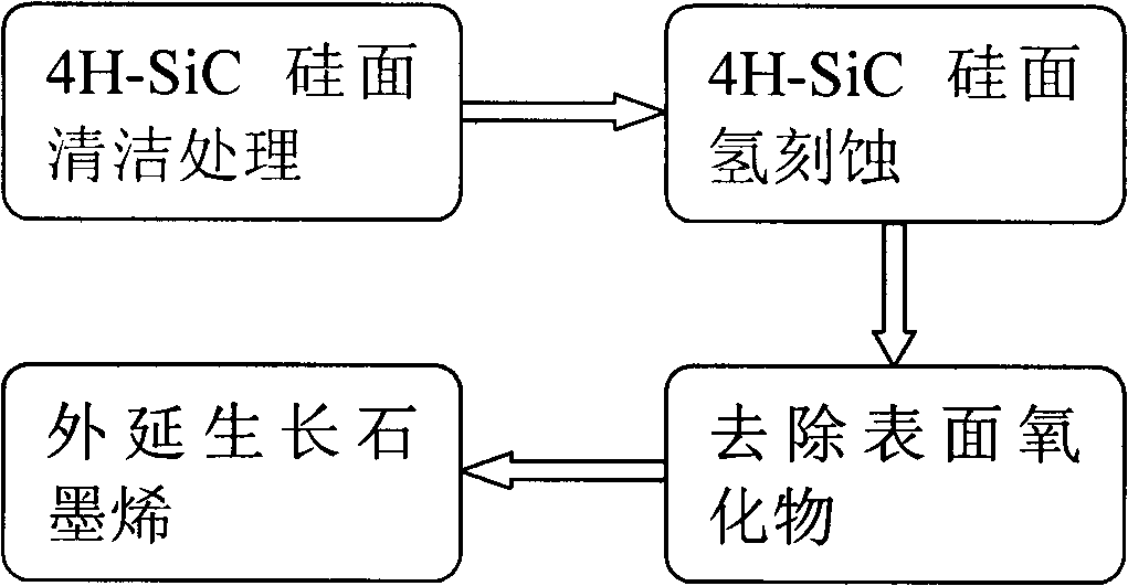
[0016] Embodiment 1, the present invention is as follows in the step of epitaxial growth of Graphene on 4H-SiC silicon surface:

[0017] The first step is to remove contaminants on the surface of the sample.

[0018] Surface cleaning of 4H-SiC silicon surface, first use NH 4 OH+H 2 O 2 Soak the sample in the reagent for 10 minutes, take it out and dry it to remove the organic residue on the surface of the sample; then use HCl+H 2 O 2 Samples were soaked in reagents for 10 minutes, removed and dried to remove ionic contaminants.

[0019] In step 2, hydrogen etching is performed on the 4H-SiC silicon surface.

[0020] Place the 4H-SiC silicon surface in a vacuum of 2.4×10 -6 In the CVD furnace chamber of mbar, hydrogen with a flow rate of 60l / min was introduced. When the temperature was raised to 1400°C, propane with a flow rate of 8ml / min was introduced. The temperature was raised to 1500°C and the pressure was 90mbar. Then take it out to remove surface scratches and for...

Embodiment 2

[0025] Embodiment 2, the steps of the present invention to epitaxially grow Graphene on the 4H-SiC silicon surface are as follows:

[0026] Step 1, remove contaminants from the sample surface.

[0027] Surface cleaning of 4H-SiC silicon surface, first use NH 4 OH+H 2 O 2 Soak the sample in the reagent for 10 minutes, take it out and dry it to remove the organic residue on the surface of the sample; then use HCl+H 2 O 2 Samples were soaked in reagents for 10 minutes, removed and dried to remove ionic contaminants.

[0028] In step 2, hydrogen etching is performed on the 4H-SiC silicon surface.

[0029] Place the 4H-SiC silicon surface in a vacuum of 2.4×10 -6 In the CVD furnace chamber of mbar, hydrogen with a flow rate of 100 l / min was introduced. When the temperature was raised to 1500 °C, propane with a flow rate of 12 ml / min was introduced. The temperature was raised to 1650 °C and the pressure was 100 mbar. Then take it out to remove surface scratches and form regul...

Embodiment 3

[0034] Embodiment 3, the present invention is as follows in the step of epitaxial growth of Graphene on 4H-SiC silicon surface:

[0035] Step A, removing contaminants on the surface of the sample.

[0036] Surface cleaning of 4H-SiC silicon surface, first use NH 4 OH+H 2 O 2 Soak the sample in the reagent for 10 minutes, take it out and dry it to remove the organic residue on the surface of the sample; then use HCl+H 2 O 2 Samples were soaked in reagents for 10 minutes, removed and dried to remove ionic contaminants.

[0037] In step B, hydrogen etching is performed on the 4H-SiC silicon surface.

[0038] Place the 4H-SiC silicon surface in a vacuum of 2.4×10 -6 In the CVD furnace chamber of mbar, hydrogen with a flow rate of 90l / min was introduced. When the temperature was raised to 1450°C, propane with a flow rate of 10ml / min was introduced, the temperature was raised to 1600°C, and the pressure was 96mbar. Then take it out to remove surface scratches and form regular s...


PUM

PropertyMeasurementUnit
densityaaaaaaaaaa

Abstract

The invention discloses a method for graphene epitaxial growth on 4H-SiC silicon surface, mainly solving the problems of small graphene area and poor homogeneity during graphene epitaxial growth on the 4H-SiC silicon surface. The method is as follows: a 4H-SiC silicon surface is cleaned to remove organic remains and ionic contaminants on the surface; hydrogen and propane are led in to carry out hydrogen corrosion to the 4H-SiC silicon surface to remove surface scratches so as to form regular step-shaped stripes; silane is led in to remove oxide formed by hydrogen corrosion on the surface; under the circumstance of argon, silicon atoms are evaporated to ensure carbon atom to reconstruct and form epitaxial graphene in the form of sp<2> by heating. The invention can be used for manufacturing epitaxial graphene materials.

Description

technical field [0001] The invention belongs to the technical field of microelectronics, and relates to the manufacture of semiconductor materials, in particular to a method for preparing graphene by epitaxial growth on a 4H-SiC (0001) plane. Background technique [0002] The silicon-based microfabrication technology marked by integrated circuits has created the contemporary information society. It is generally believed that the processing limit of silicon material is 10nm line width. Restricted by physical principles, less than 10nm is unlikely to produce products with stable performance and higher integration. Therefore, the current technological progress on silicon materials will become more and more difficult, and people are pinning their hopes on the electronics of carbon-based materials. Carbon nanotubes were the first to attract attention because of their high mobility, high thermal conductivity, and good current capability, but carbon nanotubes are difficult and re...

Claims


Application Information

Patent Timeline
Patent Type & Authority Patents(China)
IPC IPC(8): C01B31/04C30B29/02
Inventor 张玉明郭辉王党朝张义门汤晓燕王悦湖王德龙
Owner XIDIAN UNIV
Why Eureka
Try Eureka