Process for manufacturing three-layer continuous surface type MEMS deformable mirror based on bonding process

A bonding process and manufacturing process technology, applied in the field of manufacturing process of three-layer continuous surface MEMS deformable mirror, to achieve the effect of eliminating electrostatic pull-in, wide application and large off-plane displacement

Inactive Publication Date: 2009-12-16
INST OF OPTICS & ELECTRONICS - CHINESE ACAD OF SCI
View PDF0 Cites 6 Cited by
  • Summary
  • Abstract
  • Description
  • Claims
  • Application Information

AI Technical Summary

Problems solved by technology

[0003] The technical problem to be solved in the present invention is: Aiming at the deficiencies of the prior art, a manufacturing process of a three-layer continuous surface MEMS deformable mirror bas

Method used


Image

  • Process for manufacturing three-layer continuous surface type MEMS deformable mirror based on bonding process
  • Process for manufacturing three-layer continuous surface type MEMS deformable mirror based on bonding process
  • Process for manufacturing three-layer continuous surface type MEMS deformable mirror based on bonding process

Examples


Embodiment 1

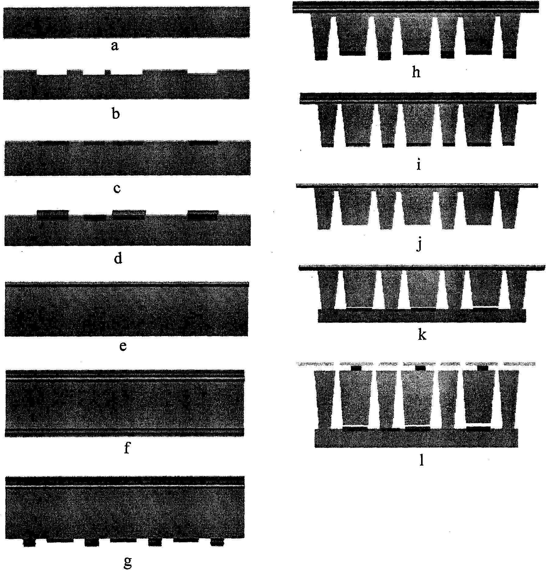
[0034] Taking the manufacturing process of a three-layer continuous surface-shaped micromechanical deformable mirror with 3 × 3 units as an example, the present invention will be described in detail in conjunction with the accompanying drawings. The specific steps are as follows: figure 1 shown.

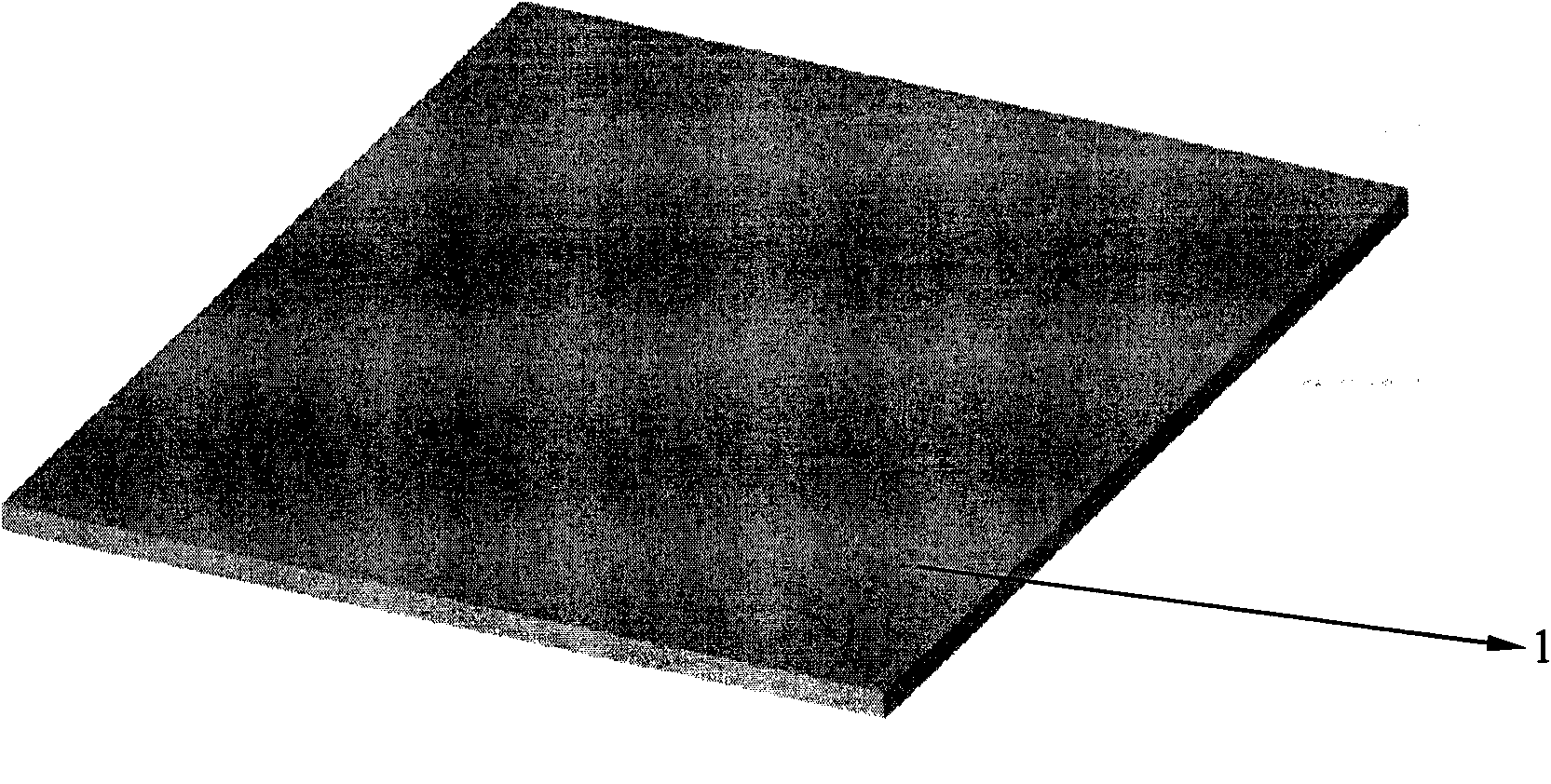
[0035] 1. Take a piece of 5-inch Pyrex7740 glass with a thickness of 500 microns as the first substrate 1, such as figure 2 shown.

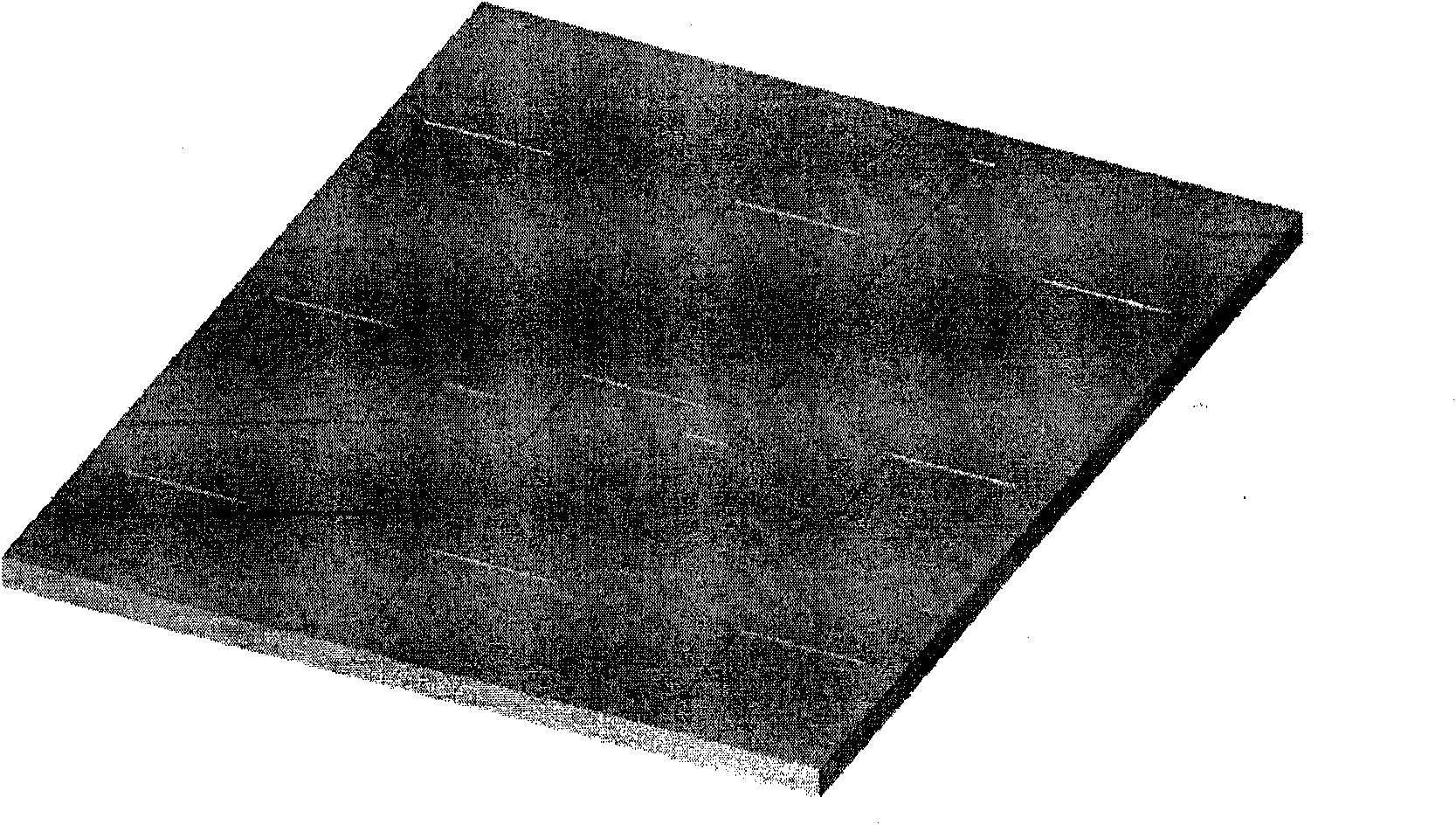
[0036] 2. Use the first mask photolithography and wet etching with buffered hydrofluoric acid to form a 0.5 micron deep groove to prepare for the deposition of the lower electrode, such as image 3 shown.

[0037] 3. Evaporate gold with a thickness of 0.5 microns on the upper surface of the glass substrate, then photolithography and dry etching, the etching depth is 0.5 microns, and form the lower electrode 3 and lead 2 of the deformable mirror, such as Figure 4 shown.

[0038] 4. Deposit a silicon nitride film 4 with a thickness of 0.5 microns by...

Embodiment 2

[0046] Taking the manufacturing process of the three-layer continuous surface-shaped micromechanical deformable mirror with 7×7 units as an example, the present invention will be described in detail in conjunction with the accompanying drawings. The specific steps are as follows: figure 1 shown.

[0047] 1. Take a 5-inch Corning 7070 glass with a thickness of 1000 microns as the first substrate 1, such as figure 2 shown.

[0048] 2. Use the first mask to lithography and wet-etch a 2 micron deep groove with buffered hydrofluoric acid to prepare for laying the lower electrode, such as image 3 shown.

[0049] 3. Evaporate gold with a thickness of 2.0 microns on the upper surface of the substrate, then photolithography and dry etching, the etching depth is 2 microns, and form the lower electrode 3 and lead 2 of the deformable mirror, such as Figure 4 shown.

[0050] 4. Deposit a silicon nitride film 4 with a thickness of 1 micron by LPCVD, then photolithography and dry etch...

Embodiment 3

[0058] Taking the manufacturing process of a 10×10 unit three-layer continuous surface-shaped micromechanical deformable mirror as an example, the present invention will be described in detail in conjunction with the accompanying drawings. The specific steps are as follows: figure 1 shown.

[0059] 1. Take a 4-inch N-type (100) double-sided polished Max silicon wafer with a thickness of 300 microns as the first substrate 1, with a resistivity of 10 5 ~2×10 5 Ω·cm, such as figure 2 shown.

[0060] 2. Use the first mask plate photolithography and wet-etch a 0.1 micron deep groove with 50% potassium hydroxide solution to prepare for laying the lower electrode, such as image 3 shown.

[0061] 3. Deposit polycrystalline silicon with a thickness of 0.1 micron by LPCVD, then photolithography and dry etching, the etching depth is 0.1 micron, to form the lower electrode 3 and lead 2 of the deformable mirror, as Figure 4 shown.

[0062] 4. Deposit a silicon nitride film 4 with ...


PUM

PropertyMeasurementUnit
Thicknessaaaaaaaaaa
Thicknessaaaaaaaaaa
Resistivityaaaaaaaaaa

Abstract

The invention discloses a process for manufacturing a three-layer continuous surface type MEMS deformable mirror based on a bonding process, which mainly comprises the following steps: performing dry-etching of a releasing hole on the upper surface of an SOI wafer, partially releasing a middle oxidation layer of the SOI wafer, performing wet-etching on the lower surface of the SOI wafer, depositing a metal on another substrate (silicon wafer or glass) as an electrode structure, and finally bonding the substrate and the SOI wafer. The process is characterized in that a bulk silicon micromachining process and a surface micromachining process are combined, and an upper two-layer structure obtained by adopting the bulk silicon process and a lower electrode structural layer obtained by adopting surface micromachining are bonded to form a three-layer micromechanical structure. The process for manufacturing the three-layer continuous surface type MEMS deformable mirror based on the bonding process has a relatively easy manufacturing process, overcomes the defect that the prior continuous surface micromechanical deformable mirror is difficult to process through three-layer surface micromachining, can eliminate the defect of short circuit due to electrostatic draw-in by adding a silicon nitride insulating layer, and can be widely applicable in the fields of optical communication and adaptive optics; and the machined deformable mirror can obtain large out-of-plane displacement.

Description

technical field [0001] The invention relates to the technical field of micro-opto-electromechanical systems, in particular to a manufacturing process of a three-layer continuous surface MEMS deformable mirror based on a bonding process suitable for an adaptive optical system. Background technique [0002] In the field of adaptive optics, electrostatically driven MEMS deformable mirrors have the advantages of small size, low power consumption, fast response, mass production, and good compatibility with integrated circuits, so they are favored in adaptive optics systems. The existing electrostatically driven MEMS deformable mirrors are generally processed by surface micromachining technology, which is difficult to process; and to obtain a large stroke, such as a stroke greater than 4 microns, due to the influence of the electrostatic pull-in effect, the stroke of the driver cannot If it exceeds one-third of the initial plate spacing, the thickness of the sacrificial layer need...

Claims


Application Information

Patent Timeline
IPC IPC(8): G02B26/08
Inventor 姚军任豪陶逢刚邱传凯
Owner INST OF OPTICS & ELECTRONICS - CHINESE ACAD OF SCI
Why Eureka
Try Eureka