Processing method of lithography machine silicon slice alignment signals

A technology of silicon wafer alignment and processing method, which is applied in the direction of microlithography exposure equipment, photolithography exposure equipment, etc., and can solve the problems of large alignment errors, etc.

Active Publication Date: 2009-12-30
SHANGHAI MICRO ELECTRONICS EQUIP (GRP) CO LTD
View PDF1 Cites 25 Cited by
  • Summary
  • Abstract
  • Description
  • Claims
  • Application Information

AI Technical Summary

Problems solved by technology

[0004] In order to solve the technical problem of large alignment errors during the processing of the silicon wafer alignment signals of the prior art lithograph

Method used


Image

  • Processing method of lithography machine silicon slice alignment signals
  • Processing method of lithography machine silicon slice alignment signals
  • Processing method of lithography machine silicon slice alignment signals

Examples


Embodiment Construction

[0027] In order to make the object, technical solution and advantages of the present invention clearer, the present invention will be further described in detail below in conjunction with the accompanying drawings.

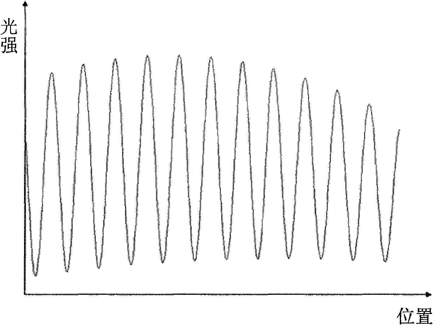
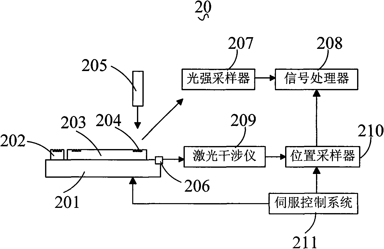
[0028] see figure 2 . A schematic diagram of a silicon wafer alignment system of a photolithography machine using the method for processing silicon wafer alignment signals of a photolithography machine according to the present invention. The silicon wafer alignment system 20 of the lithography machine includes a workpiece table 201, which can freely reciprocate in the horizontal direction; a reference plate 202 and a silicon wafer 203 attached to the workpiece table 201; 202 and the alignment marks 204 on the silicon wafer 203; a laser light source 205 for providing alignment illumination; a light intensity sampler 207 for converting the alignment optical signal into a digital electrical signal; for determining the position of the workpiece table 201 The mirror ...


PUM


Abstract

The invention relates to a processing method of lithography machine alignment signals, comprising the following steps: setting a non-linear model for processing the alignment signals of the lithography machine silicon slice; carrying out alignment scanning on the lithography machine silicon slice to obtain position sampling data and light intensity sampling data; carrying out real-time accumulative processing on the position sampling data and the light intensity sampling data to obtain accumulation coefficient; confirming non-linear parameter initial value of the non-linear model according to a linear model containing dark current, sine coefficient and cosine coefficient; obtaining the linear parameters of the non-linear model according to the accumulation coefficient and the non-linear parameter; obtaining iteration increment of the non-linear parameter according to the accumulation coefficient and the linear parameters of the non-linear model; updating the non-linear parameters of the non-linear model according to the iteration increment; judging whether the iteration increment meets accuracy requirement so as to determine the final linear parameters and the final non-linear parameters of the non-linear model.

Description

technical field [0001] The invention relates to a method for processing silicon chip alignment signals of a photolithography machine. Background technique [0002] Overlay accuracy is one of the key indicators of the lithography machine. In order to achieve higher overlay accuracy, it is necessary to accurately establish the relationship between the coordinate systems of the lithography machine. Off-axis alignment is the alignment between the diffraction mark formed by the reflected light of the polarized laser irradiated on the silicon wafer mark and the reference mark of the silicon wafer after diffraction, because the silicon wafer mark is attached to the silicon wafer or the silicon wafer stage , the alignment scan between the alignment mark and the reference mark can be formed by moving the workpiece table at a constant speed, and the precise alignment position can be obtained by signal processing the synchronously sampled light intensity and data. [0003] Chinese pat...

Claims


Application Information

Patent Timeline
IPC IPC(8): G03F7/20
Inventor 陈延太宋海军李运锋
Owner SHANGHAI MICRO ELECTRONICS EQUIP (GRP) CO LTD
Why Eureka
Try Eureka