Thin film production method

A thin-film manufacturing method and thin-film layer technology are applied in the field of thin-film manufacturing, which can solve the problems of decreased product yield, decreased accuracy and uniformity of thin-film thickness, and it is not easy to produce shallow implantation of good ion distribution, achieving uniform thickness, The effect of extensive use of value

Inactive Publication Date: 2010-01-06
李 天锡
View PDF2 Cites 13 Cited by
  • Summary
  • Abstract
  • Description
  • Claims
  • Application Information

AI Technical Summary

Problems solved by technology

[0010] Afterwards, the surface of the target substrate is etched, and the excess silicon on the etch stop layer is removed, so that the ultra-thin single crystal silicon layer and the etch stop layer remain on the target substrate, and are reused to manufacture bonded back-etched silicon crystals. Insulator method to produce ultra-thin silicon insulator wafers, but still has the disadvantage of uneven film thickness
[0011] Based on the above, it is not easy to produce shallow implants with good ion distribution due to the light weight of hydrogen ions in the production of silicon insulators by the smart cutting method, which makes it difficult for the thickness of the transferred film to reach the nanometer level.
In addition, the film thickness of the transferred film needs further thinning steps to

Method used


Image

  • Thin film production method
  • Thin film production method
  • Thin film production method

Examples


Embodiment Construction

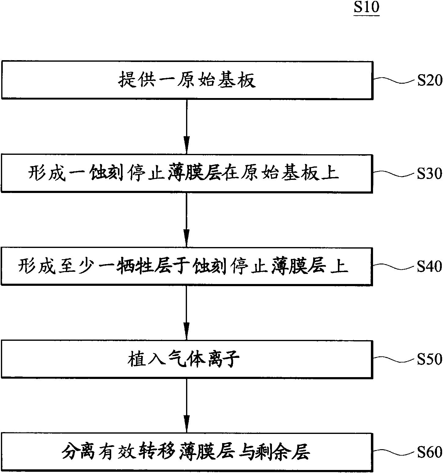
[0068] In order to further illustrate the technical means and effects that the present invention takes to achieve the intended purpose of the invention, below in conjunction with the accompanying drawings and preferred embodiments, the specific implementation methods, methods, steps, features and features of the thin film manufacturing method proposed according to the present invention will be described below. Efficacy, detailed as follows.

[0069] The aforementioned and other technical contents, features and effects of the present invention will be clearly presented in the following detailed description of preferred embodiments with reference to the drawings. For convenience of description, in the following embodiments, the same elements are denoted by the same numbers.

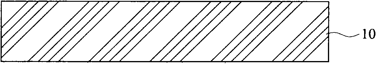
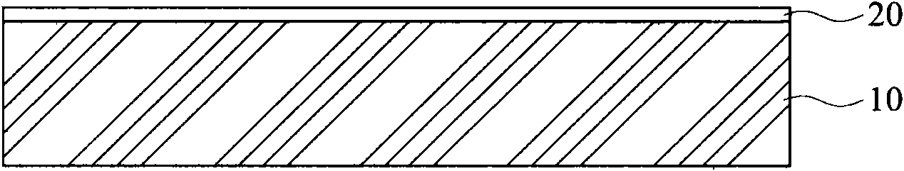
[0070] figure 1 It is an embodiment of a thin film manufacturing method S10 flow process of the present invention Figure 1 . 2A Figure to Figure 2F it's for figure 1 An example diagram of the process...


PUM


Abstract

The invention relates to a thin film production method comprising the following steps: providing an original substrate; forming a etching ceasing thin film on the original substrate; forming a sacrificial layer on the etching ceasing thin film; embedding gas ion to form an ion distribution concentration peak layer and define an effective transferring thin film and a residual layer; and separating the effective transferring thin film and the residual layer. The thickness of the effective transferring thin film can be effectively controlled by controlling the thickness of the sacrificial layer. In addition, the thickness of the effective transferring thin film is even and reaches the nanoscale thickness.

Description

technical field [0001] The invention relates to a thin film manufacturing method, in particular to a manufacturing method for synthesizing a thin film on a substrate. Background technique [0002] Silicon On Insulator (Silicon On Insulator, SOI) is mainly to set an insulating layer under the silicon wafer to avoid electrical effects and reduce power consumption to reduce current loss. In addition, Silicon On Insulator can also speed up the integrated circuit (Integrated Circuit , IC) processing speed. Silicon insulators can be used in devices that require low power consumption, such as mobile phones, watches, etc. In order to fully utilize the characteristics of high-speed operation of silicon insulators, they are also actively developing for high-frequency integrated circuits. [0003] There are also various manufacturing methods for silicon crystal insulators, which will be described as follows. In 1988, Dr. W. Maszara in the United States used an etch stop layer (Etch S...

Claims


Application Information

Patent Timeline
IPC IPC(8): H01L21/00H01L21/02H01L21/265H01L21/20H01L21/762H01L21/84H01L21/336
Inventor 李天锡黄敬涵张朝喨杨耀渝
Owner 李 天锡
Why Eureka
Try Eureka