

Method for plating thick gold layer in circuit board manufacturing process
A circuit board manufacturing and circuit board technology, applied in the directions of printed circuit manufacturing, printed circuits, electrical components, etc., can solve the problems of difficult control of gold, poor electroplating resistance, easy penetration and plating, etc., and achieve surface treatment without pollution and surface treatment. Good effect with good plating resistance
- Summary
- Abstract
- Description
- Claims
- Application Information
AI Technical Summary
Problems solved by technology
Method used
Image

Examples
Embodiment 1
[0049] Embodiment 1, a kind of thick gold plating method in the circuit board manufacturing process comprises the following steps:
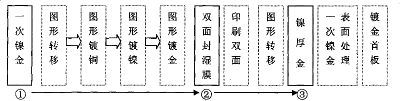
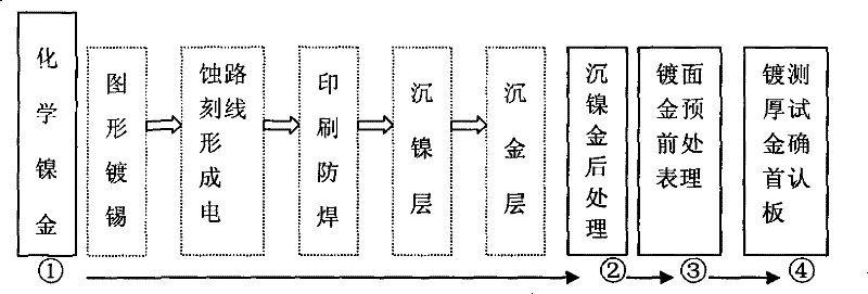
[0050] A. First, carry out chemical nickel-gold treatment on the circuit board with graphic tin plating, etching circuit lines, printing solder mask, immersion nickel layer, and immersion gold layer;
[0051] The graphic tin plating includes the following steps:
[0052] a1. Copper plating after drilling holes on the cut circuit board, wherein the circuit board is immersed in the copper plating solution for copper plating, and the copper plating solution CU 2+ The concentration is: 60 grams of CU per liter of solution 2+ , CL - : 40ppm, containing H in every 100 liters of solution 2 SO 4 8 liters;
[0053] b1. After copper plating, pre-treat the grinding plate, then print the wet film or paste the dry film, then bake the plate, align, expose and develop the wet film or dry film, and then produce graphics;
[0054] c1, and then copper electr...
Embodiment 2
[0081] Embodiment 2, a kind of thick gold plating method in circuit board manufacturing process, comprises the following steps:
[0082] A. First, carry out chemical nickel-gold treatment on the circuit board with graphic tin plating, etching circuit lines, printing solder mask, immersion nickel layer, and immersion gold layer;
[0083] The graphic tin plating includes the following steps:
[0084] a1. Copper plating after drilling holes on the cut circuit board, wherein the circuit board is immersed in the copper plating solution for copper plating, and the copper plating solution CU 2+ The concentration is: 80 grams of CU per liter of solution 2+ , CL - : 80ppm, every 100 liters of solution contains H 2 SO 4 10 liters;
[0085] b1. After copper plating, pre-treat the grinding plate, then print the wet film or paste the dry film, then bake the plate, align, expose and develop the wet film or dry film, and then produce graphics;
[0086] c1, and then copper electroplatin...
Embodiment 3
[0113] Embodiment 3, a kind of thick gold plating method in the circuit board manufacturing process comprises the following steps:
[0114] A. First, carry out chemical nickel-gold treatment on the circuit board with graphic tin plating, etching circuit lines, printing solder mask, immersion nickel layer, and immersion gold layer;
[0115] The graphic tin plating includes the following steps:
[0116] a1. Copper plating after drilling holes on the cut circuit board, wherein the circuit board is immersed in the copper plating solution for copper plating, and the copper plating solution CU 2+ The concentration is: 70 grams of CU per liter of solution 2+ , CL - : 60ppm, every 100 liters of solution contains H 2 SO 4 12 liters;
[0117] b1. After copper plating, pre-treat the grinding plate, then print the wet film or paste the dry film, then bake the plate, align, expose and develop the wet film or dry film, and then produce graphics;
[0118] c1, and then copper electropla...
PUM
 Abstract
Description
Claims
Application Information