

Conducting film integrated structure
A technology integrating structure and conductive film, which is applied in the input/output process of electrical digital data processing, instruments, and data processing, etc., can solve the problems of ITO surface cracking or fragmentation, and achieves omitting the surface concave and convex shape and extremely complex structure, Stable use effect and durable effect
- Summary
- Abstract
- Description
- Claims
- Application Information
AI Technical Summary
Problems solved by technology
Method used
Image

Examples
Embodiment Construction
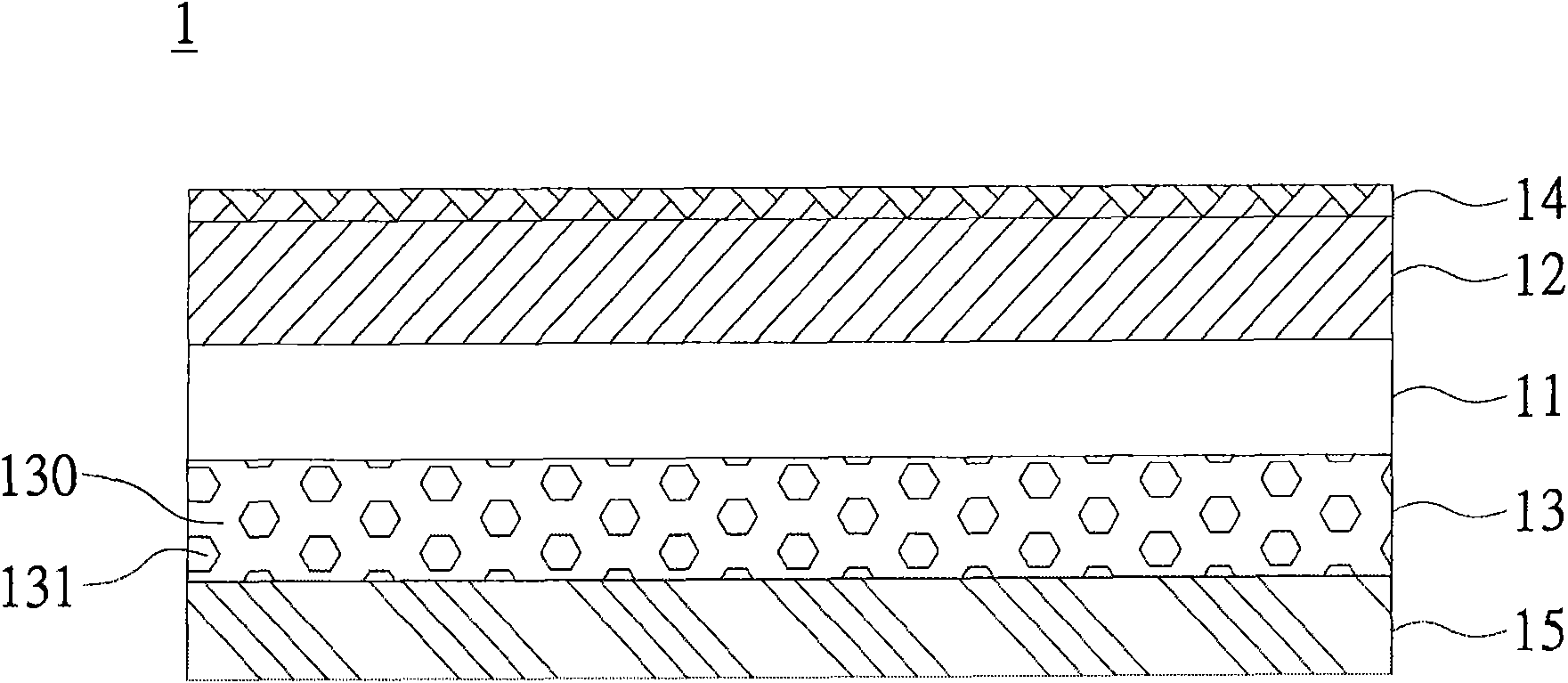
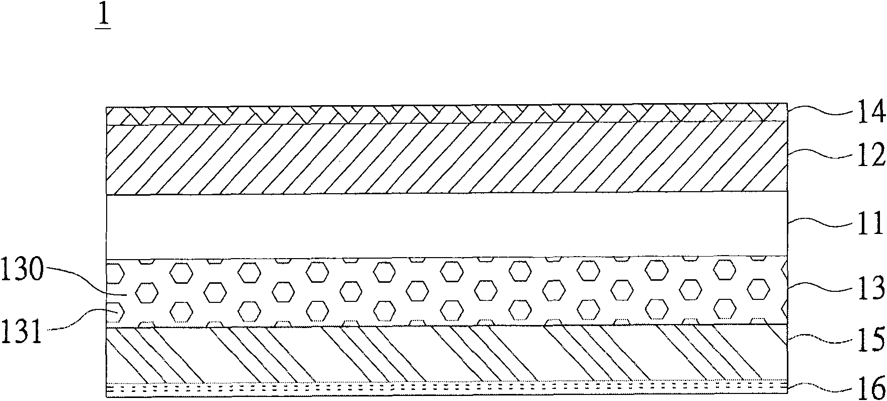
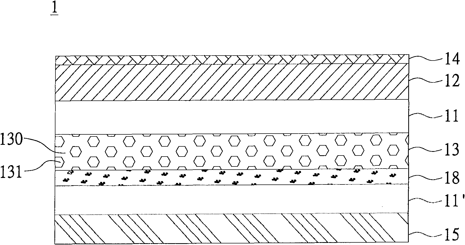
[0035] see figure 1 Shown is a schematic view of the first embodiment of the conductive film integrated structure 1 of the present invention. The conductive film integrated structure 1 of this embodiment includes: a substrate 11, an anti-glare layer (Anti-Glare Layer, AG) 12, an anti-Newton (Anti-Newton ring Layer, ANR) ring layer 13, a hard layer 14, and a transparent conductive film 15.
[0036] The substrate 11 is a transparent resin, which is polyethylene terephthalate (PET), cellulose triacetate (TAC), polyethylene naphthalate (PEN), polypropylene glycol, polyimide Amine, polyether, polycarbonate, polyamine, polyethylene, polypropylene or polyvinyl alcohol, polystyrene, polymethyl methacrylate, polyvinyl chloride, epoxy resin, phenolic resin, etc. or their equivalents.
[0037] The anti-glare layer 12 is arranged on one side of the base material 11, and the surface of the anti-glare layer 12 has a light-guiding microstructure (not shown), which is used to increase the d...
PUM
| Property | Measurement | Unit |
|---|---|---|
| Thickness | aaaaa | aaaaa |
| Size | aaaaa | aaaaa |
| Thickness | aaaaa | aaaaa |
Abstract
Description
Claims
Application Information