Optical compensation birefringence liquid crystal box and manufacture method thereof
A technology of optical compensation and manufacturing method, applied in optics, nonlinear optics, instruments, etc., can solve the problems of complicated process, high operating voltage, high conversion voltage, etc. Effect
- Summary
- Abstract
- Description
- Claims
- Application Information
AI Technical Summary
Problems solved by technology
Method used
Image
Examples
experiment example 1
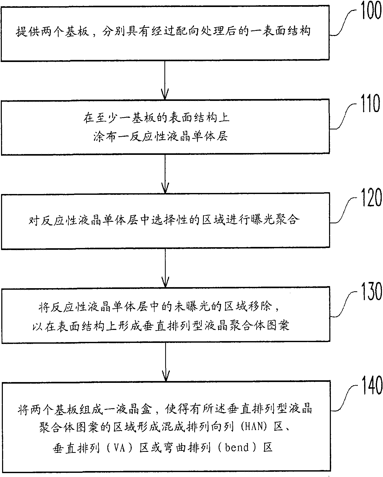
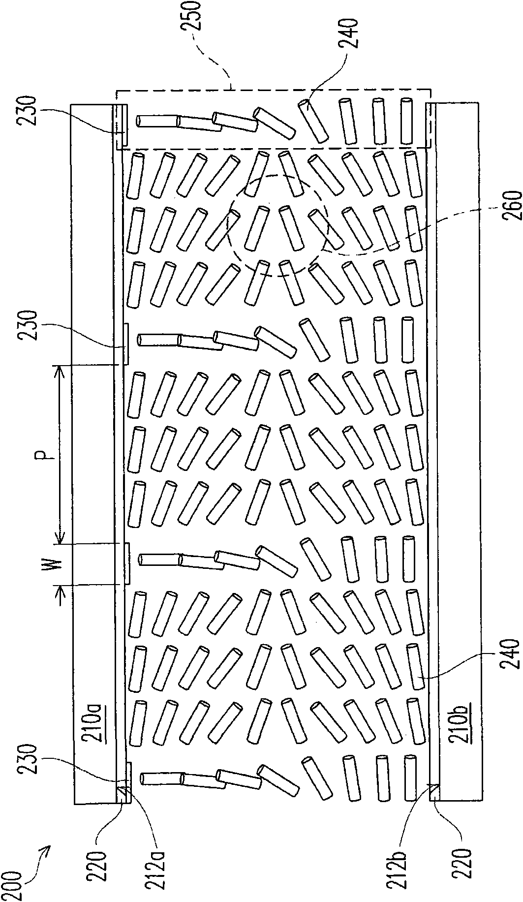
[0063] First, a surface alignment film (PIA-5560-05A, Chisso) of a glass substrate was rubbed and then coated with a reactive liquid crystal monomer layer with a thickness of about 100 angstroms on the surface structure. Then, by means of UV exposure, the partial area of the reactive liquid crystal monomer layer is selectively polymerized (polymerizing), and then the surface structure is cleaned with a solvent such as methyl ethyl ketone, and the reactive liquid crystal monomer layer that has not been polymerized by UV light is polymerized. removed, leaving behind a polymerized liquid crystal polymer (LCP) pattern (such as Image 6 shown). exist Image 6The liquid crystal polymer pattern is perpendicular to the alignment direction, and has linear structures 600 with a line width of about 5 μm, and the distance between the linear structures 600 is about 90 μm. Then, a piece of the glass substrate after the above treatment and the alignment substrate without the above treatm...
experiment example 2
[0068] Using the method of Experimental Example 1, a liquid crystal polymer pattern was formed on the rubbed-aligned surface structure, and the difference from Experimental Example 1 was that the line width of the linear structure was 10 μm.
experiment example 3
[0070] Using the method of Experimental Example 1, a liquid crystal polymer pattern was formed on the rubbed-aligned surface structure, and the difference from Experimental Example 1 was that the line width of the linear structure was 20 μm.
[0071] Figure 8 It is the V-T curve of the OCB type liquid crystal cell of the experimental examples 1 to 3 of the present invention. from Figure 8 It can be seen that the line width of the linear structure of the liquid crystal polymer pattern can still achieve the effect of not needing to switch from the splay state to the bend state with a slight change in the same spacing. Therefore, the method of the present invention has a wider range of process parameters (Process Window).
[0072] In addition, the above-mentioned vertical alignment liquid crystal polymer pattern can also be applied to the production of seed crystals, such as Figure 9 shown.
[0073] Figure 9 It is a top view of a partial structure of an optically compens...
PUM
| Property | Measurement | Unit |
|---|---|---|
| Thickness | aaaaa | aaaaa |
| Radius | aaaaa | aaaaa |
| Thickness | aaaaa | aaaaa |
Abstract
Description
Claims
Application Information
 - R&D Engineer
- R&D Manager
- IP Professional
- Industry Leading Data Capabilities
- Powerful AI technology
- Patent DNA Extraction
Browse by: Latest US Patents, China's latest patents, Technical Efficacy Thesaurus, Application Domain, Technology Topic, Popular Technical Reports.
© 2024 PatSnap. All rights reserved.Legal|Privacy policy|Modern Slavery Act Transparency Statement|Sitemap|About US| Contact US: help@patsnap.com


