Structure and method for improving current crowding effect of microwave power transistor emitter region

A technology of microwave power and emission area, applied in the direction of transistors, circuits, electrical components, etc., can solve the problems of limiting chip output power, reducing the width of the emission area, affecting the processing yield, etc., to reduce the difference in voltage drop, Reduce process difficulty and improve the effect of microwave output power

Inactive Publication Date: 2010-02-03
NO 55 INST CHINA ELECTRONIC SCI & TECHNOLOGYGROUP CO LTD
View PDF0 Cites 11 Cited by
  • Summary
  • Abstract
  • Description
  • Claims
  • Application Information

AI Technical Summary

Problems solved by technology

However, this design is not conducive to reducing the collector area, which limits the output power per unit area of ​​th

Method used


Image

  • Structure and method for improving current crowding effect of microwave power transistor emitter region
  • Structure and method for improving current crowding effect of microwave power transistor emitter region
  • Structure and method for improving current crowding effect of microwave power transistor emitter region

Examples


Embodiment 1

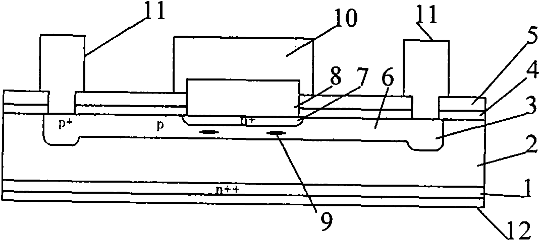
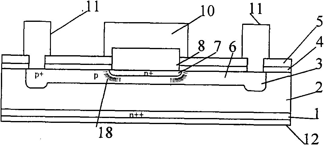
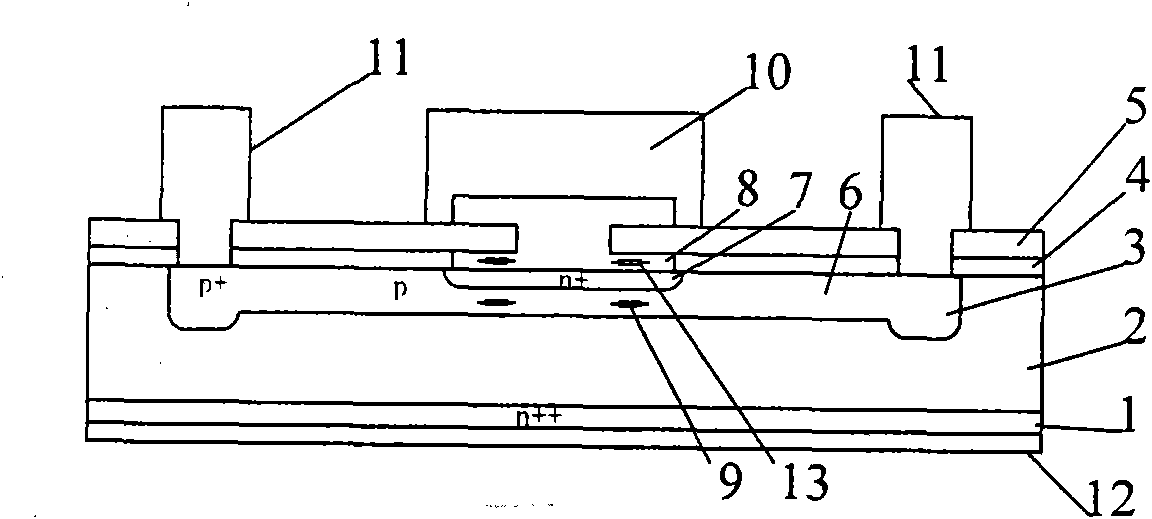
[0058] 1) Select an arsenic-doped silicon substrate region with a thickness of 380 μm and a resistivity of ≤0.003Ω·cm, and its silicon epitaxial layer is doped with phosphorus (n-type), with a resistivity of 0.75Ω·cm and a thickness of 1 μm (attached Figure 5 );

[0059] 2) Coating a layer of photoresist film on the surface of the silicon substrate with a thickness of 1.0 μm (attached Figure 6 );

[0060] 3) Selectively expose and develop the photoresist to obtain a window in the base contact area, and then perform B in the window by using an ion implantation process. + (or BF 2 + ) doping to form p + doped region (attached Figure 7 );

[0061] 4), using dry or wet process to remove the attached Figure 5 The photoresist in the photoresist, and then re-coat a layer of photoresist film on the surface of the silicon substrate, with a thickness of 1.0 μm; selectively expose and develop the photoresist to form a base injection window (attached Figure 8 );

[0062] 5) Pe...

Embodiment 2

[0074] 1) Select an arsenic-doped silicon substrate region with a thickness of 470 μm and a resistivity of ≤0.003Ω·cm, and its silicon epitaxial layer is doped with phosphorus (n-type), with a resistivity of 1.125Ω·cm and a thickness of 8 μm (attached Figure 5 );

[0075] 2) Coating a layer of photoresist film on the surface of the silicon substrate with a thickness of 1.75 μm (attached Figure 6 );

[0076] 3) Selectively expose and develop the photoresist to obtain a window in the base contact area, and then perform B in the window by using an ion implantation process. + (or BF 2 + ) doping to form p + doped region (attached Figure 7 );

[0077] 4), using dry or wet process to remove the attached Figure 5 The photoresist in the photoresist, and then re-coat a layer of photoresist film on the surface of the silicon substrate, with a thickness of 1.75 μm; selectively expose and develop the photoresist to form a base injection window (attached Figure 8 );

[0078] 5)...

Embodiment 3

[0088] 1) Select an arsenic-doped silicon substrate region with a thickness of 560 μm and a resistivity of ≤0.003Ω·cm, whose silicon epitaxial layer is doped with phosphorus (n-type), with a resistivity of 1.5Ω·cm and a thickness of 15 μm (attached Figure 5 );

[0089] 2) Coating a layer of photoresist film on the surface of the silicon substrate with a thickness of 2.5 μm (attached Figure 6 );

[0090] 3) Selectively expose and develop the photoresist to obtain a window in the base contact area, and then perform B in the window by using an ion implantation process. + (or BF 2 + ) doping to form p + doped region (attached Figure 7 );

[0091] 4), using dry or wet process to remove the attached Figure 5 The photoresist in the photoresist, and then re-coat a layer of photoresist film on the surface of the silicon substrate, with a thickness of 2.5 μm; selectively expose and develop the photoresist to form a base injection window (attached Figure 8 );

[0092] 5) Perf...


PUM

PropertyMeasurementUnit
Thicknessaaaaaaaaaa
Resistivityaaaaaaaaaa

Abstract

The invention relates to a structure and a method for improving the current crowding effect of a microwave power transistor emitter region. The structure is characterized in that the emitter region isprovided with a polysilicon thin-layer distribution resistor which is parallel to the surface of a silicon substrate and an emitter junction for balancing a distribution resistor of a base region below the emitter region and improving the voltage consistency of the emitter junction so as to improve the current crowding effect of the emitter region; and the thin-layer distribution resistor of theemitter region is made of doped polysilicon and acquires a resistor value of the needed doped polysilicon resistor by controlling the thickness and the side undercutting depth of silicon dioxide forming a window of the emitter region. The invention has the advantages that the polysilicon thin-layer distribution resistor parallel to the surface of the silicon substrate and the emitter junction is led in the emitter region; and when a current of the emitter region flows by the distributed resistor, a generated voltage drop compensates the voltage drop of a base current on an inner base resistor,reduces the voltage drop differences of the emitter junction in different positions, improves the current crowding effect, expands the effective working area of the emitter junction and improves themicrowave output power of a chip unit area.

Description

technical field [0001] The invention relates to a structure and method for improving the current edge-collection effect in the emitting area of ​​the microwave power transistor, which is especially suitable for the development and production of the microwave power transistor, and belongs to the technical field of semiconductor microelectronic design and manufacture. Background technique [0002] In semiconductor microwave power transistors, the resistivity of the base region below the emitter region (the so-called inner base region) is relatively high, and the width of the base region is narrow, so the resistance of the inner base region is relatively large. Due to the existence of the base resistance, when the emitter junction is in the forward biased state, the emitter junction current is mainly concentrated on the edge of the emitter junction (the so-called emitter current edge effect), and the middle region of the emitter junction only increases the emitter junction capac...

Claims


Application Information

Patent Timeline
IPC IPC(8): H01L29/73H01L29/12H01L21/331
Inventor 傅义珠
Owner NO 55 INST CHINA ELECTRONIC SCI & TECHNOLOGYGROUP CO LTD
Why Eureka
Try Eureka