Device and process method for filling aluminum into nano through holes by using PVD method

A process method and nano-scale technology, applied in metal material coating process, ion implantation plating, coating, etc., can solve the problems of high production equipment requirements, imperfect technical nodes, difficult to fill aluminum technology extension, etc., and it is not easy to achieve Breakdown, improve equipment utilization, reduce the effect of water and electricity consumption

Inactive Publication Date: 2011-07-27
吉和林
View PDF0 Cites 0 Cited by
  • Summary
  • Abstract
  • Description
  • Claims
  • Application Information

AI Technical Summary

Problems solved by technology

The second is that the aluminum filling process of the through hole is not perfect at the technical node below 0.18 microns
[0008] If the second step is made by CVD method, the CVD is uniform in all directions, but the reaction speed is slow, so it is not suitable for the third step, so two different reaction chambers are still needed
In addition, in the second step of CVD method, the carbon content of the film is high, which easily leads to the formation of voids.
[0009] All in all, the disadvantages of the prior art method are: void defects are unavoidable in the IC production process with a characteristic line width of less than 0.18 μm and a high aspect ratio, and two reaction chambers are necessary to complete the process of the second to fourth steps, and the production High equipment requirements are usually replaced by copper, which greatly increases the production cost, especially it is more difficult to extend the aluminum filling technology to below 0.1μm (nanoscale)

Method used


Image

  • Device and process method for filling aluminum into nano through holes by using PVD method
  • Device and process method for filling aluminum into nano through holes by using PVD method
  • Device and process method for filling aluminum into nano through holes by using PVD method

Examples


Embodiment Construction

[0056] The present invention is described in detail below with reference to the accompanying drawings, but they do not limit the present invention in any way.

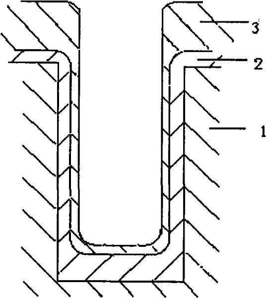
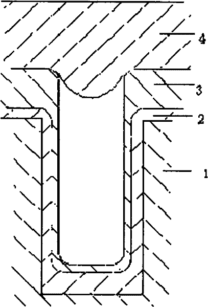
[0057] As shown in the figure, 1 is an insulator, 2 is a barrier layer, 3 is a seed layer, and 4 is aluminum.

[0058] 11 is a wafer, 22 is a target material, 33 is a magnet, 44 is a DC power supply, 55 is a wafer base, 66 is a radio frequency power supply (I), and 77 is a radio frequency power supply (II).

[0059] The device of the present invention mainly includes: a PVD chamber, a DC power supply 44, a magnet 33, a wafer base 55, a target 22, the target 22 is placed on the top of the PVD chamber, the wafer base 55 is placed on the bottom of the PVD chamber, and Opposite to the wafer base 55, a radio frequency power source (I) 66 is added to the target 22, and a radio frequency power source (II) 77 is added to the wafer (silicon chip). See Figure 7 .

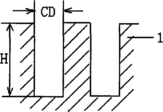
[0060] The present invention provides a nano-scale through-h...


PUM

PropertyMeasurementUnit
sizeaaaaaaaaaa

Abstract

The invention relates to a device and a process method for filling aluminum into nano through holes by using a PVD method, which adopt a radio-frequency power supply and a high-frequency plasma method of physical vapor deposition (PVD), wherein in a PVD chamber, the radio-frequency power supply is applied to a target material and a wafer respectively, and the Al is filled into the through holes of a minisize semiconductor chip and becomes a conducting material between semiconductor layers. The device and the process method can overcome the defect that the conventional process can only reach over 0.13 micron, and extend the application of the aluminum to a degree that the characteristic line width is less than or equal to 0.1 mum and the depth-to-width ratio (h / CD) is more than or equal to6. The device and the process method reduce the device running temperature, save water, electricity and consumptive materials, greatly improve the utilization rate of production facilities and the wafer yield, can be applied to the conductive through holes between semiconductor integrated circuit chip layers, contact holes, grooves and the like for filling the conductive materials of the aluminumand the like, and also can be used for depositing the aluminum used on metal door circuits of which the line width is less than 30 nanometers. The invention particularly points out that the same method is suitable for all technical materials with low melting point.

Description

technical field [0001] The present invention relates to the manufacture of VLSI chips, in particular to a device and process method for filling aluminum in nanoscale through-holes by PVD method, specifically using a radio frequency (Radio Frequency, RF) power supply and physical vapor deposition (PVD) high The high-frequency plasma method fills Al into the through holes of small-sized semiconductor chips to become a conductive material between semiconductor layers, which can overcome the defect that the traditional process can only reach 0.13 microns or more. The present invention can extend the application of aluminum to the characteristic line width≤0.1μm, and the ratio of depth to width (h / CD, Critical Dimension)≥6. Background technique [0002] VLSI (Integrated Circμit, abbreviation: IC) chip manufacturing technology develops rapidly. With the development of wafer processing to higher chip density, the size of silicon wafers used reaches 300mm or more, and the feature s...

Claims


Application Information

Patent Timeline
Patent Type & Authority Patents(China)
IPC IPC(8): C23C14/28C23C14/54
Inventor 吉和林
Owner 吉和林
Why Eureka
Try Eureka