Soft support bridge type silicon micro-piezoelectric ultrasonic transducer chip and prepration method thereof
A technology of ultrasonic transducers and soft support bridges, applied in the manufacture/assembly of piezoelectric/electrostrictive devices, piezoelectric/electrostrictive/magnetostrictive devices, zero of piezoelectric devices or electrostrictive devices Parts and other directions can solve the problem of low sensitivity of ultrasonic transducers
- Summary
- Abstract
- Description
- Claims
- Application Information
AI Technical Summary
Problems solved by technology
Method used
Image
Examples
Embodiment 1
[0092] Embodiment 1, using the preparation method of the present invention to prepare a novel piezoelectric ultrasonic transducer chip, the steps are as follows:
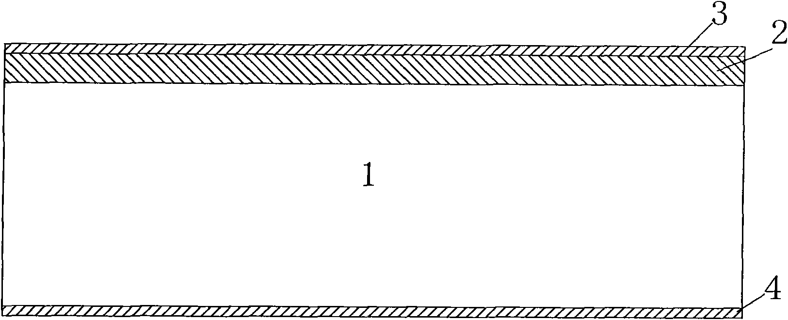
[0093] 1) Clean the silicon substrate 1
[0094] Cleaning the silicon substrate 1 with an acid cleaning solution and an alkaline cleaning solution respectively, and then rinsing it with deionized water;
[0095] 2) Formation of the B diffusion barrier by thermal oxidation
[0096] On the silicon substrate 1, use a thermal oxidation furnace to oxidize an oxide layer with a thickness of 1 μm, and remove the oxide layer on the front side, so that an oxide film layer with a thickness of 1 μm is formed on the back side of the substrate 1;
[0098] Carry out boron diffusion on the silicon substrate 1 in a diffusion furnace, and then perform oxidation treatment after the diffusion, and form B-silicate glass on the surface of the silicon substrate 1, and use buffered HF to remove the B-silicon ...
Embodiment 2
[0118] Embodiment 2, using the preparation method of the present invention to prepare a novel piezoelectric ultrasonic transducer chip, the steps are as follows:
[0119] 1) Clean the SOI substrate
[0120] Clean the SOI substrate with acid cleaning solution and alkaline cleaning solution respectively, and then rinse it with deionized water;
[0121] 2) Preparation of oxide layer
[0122] Oxidize the SOI substrate in an oxidation furnace to form a first oxide layer 3 with a thickness of 0.3 μm on the front of the substrate, and a second oxide layer 4 with a thickness of 0.3 μm on the back;
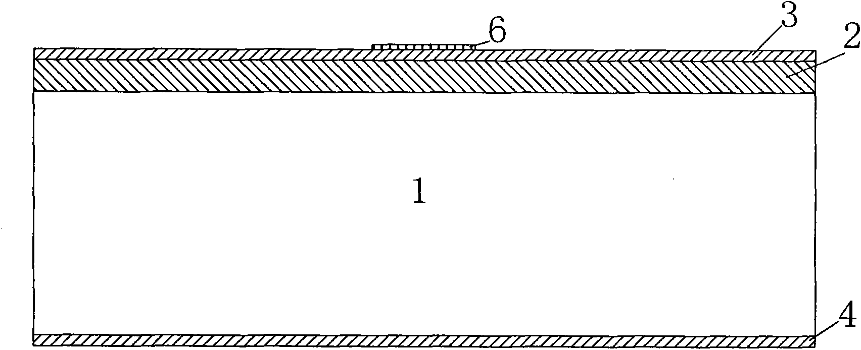
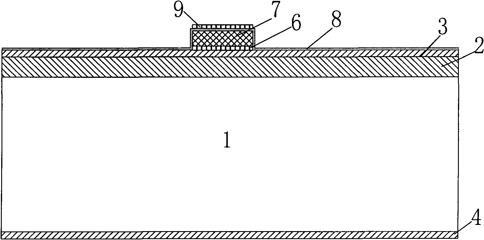
[0123] 3) Prepare the lower electrode 6
[0124] On the first oxide layer 3, use magnetron sputtering equipment to prepare a Ti layer with a thickness of 0.04 μm and a Pt layer with a thickness of 0.2 μm to form a lower electrode composite layer, and use patterning technology to form a lower electrode 6; complete the lower electrode 6 preparation;
[0125] 4) Preparation of piezoelectr...
Embodiment 3
[0140] Embodiment 3, using the preparation method of the present invention to prepare a novel piezoelectric ultrasonic transducer chip, the steps are as follows:
[0141] 1) Clean the SOI substrate
[0142] Clean the SOI substrate with acid cleaning solution and alkaline cleaning solution respectively, and then rinse it with deionized water;
[0143] 2) Preparation of oxide layer
[0144] Oxidize the SOI substrate in an oxidation furnace to form a first oxide layer 3 with a thickness of 0.3 μm on the front of the substrate, and a second oxide layer 4 with a thickness of 0.3 μm on the back;
[0145] 3) Prepare the lower electrode 6
[0146] On the first oxide layer 3, use magnetron sputtering equipment to prepare a Ti layer with a thickness of 0.04 μm and a Pt layer with a thickness of 0.2 μm to form a lower electrode composite layer, and use patterning technology to form a lower electrode 6; complete the lower electrode 6 preparation;
[0147] 4) Preparation of piezoelectric...
PUM
| Property | Measurement | Unit |
|---|---|---|
| Thickness | aaaaa | aaaaa |
| Thickness | aaaaa | aaaaa |
| Thickness | aaaaa | aaaaa |
Abstract
Description
Claims
Application Information


