Semiconductor structure and thin-film photovoltaic device having same

A thin-film photovoltaic and photovoltaic device technology, applied in semiconductor devices, photovoltaic power generation, electrical components and other directions, can solve the problems of low photoelectric conversion rate of photovoltaic devices, uneven density of germanium atoms, uneven composition, etc., to improve the light absorption rate, The effect of improving photoelectric conversion efficiency and high photocurrent

Inactive Publication Date: 2010-02-17
GS SOLAR FU JIAN COMPANY +1
View PDF0 Cites 7 Cited by
  • Summary
  • Abstract
  • Description
  • Claims
  • Application Information

AI Technical Summary

Problems solved by technology

Therefore, in a large-scale plasma chemical vapor deposition (PECVD) reactor, the spatial distribution of the reactive components containing silicon molecules and the active components containing germanium molecules is different, which makes large-area deposited amorphous silicon The density (composition) of germanium atoms in germanium thin films is not uniform, resulting in low photoelectric conversion efficiency of large-area photovoltaic devices containing intrinsic amorphous silicon germanium alloy absorber layers
In addition, as the growth rate of amorphous silicon germanium alloy increases, the problem of uneven composition gradually worsens

Method used


Image

  • Semiconductor structure and thin-film photovoltaic device having same
  • Semiconductor structure and thin-film photovoltaic device having same
  • Semiconductor structure and thin-film photovoltaic device having same

Examples


Embodiment Construction

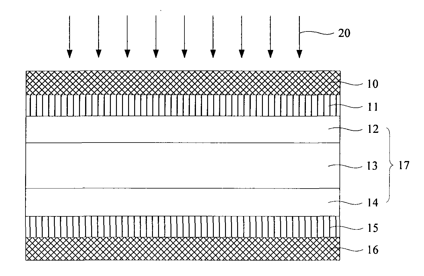
[0045] In order to make the above objects, features and advantages of the present invention more comprehensible, specific implementations of the present invention will be described in detail below in conjunction with the accompanying drawings. In the following description, numerous specific details are set forth in order to provide a thorough understanding of the present invention. However, the present invention can be implemented in many ways other than those described here, and those skilled in the art can make similar extensions without departing from the connotation of the present invention. Accordingly, the invention is not limited to the specific implementations disclosed below.

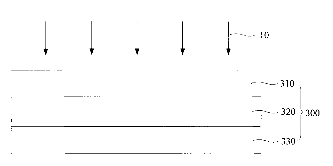
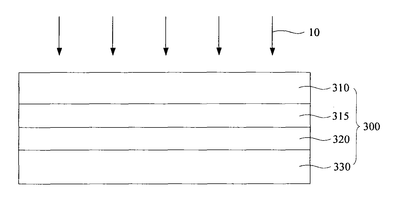
[0046] The amorphous silicon, amorphous silicon germanium, nanocrystalline silicon and amorphous germanium mentioned below all refer to hydrogenated materials of these substances, namely hydrogenated amorphous silicon, hydrogenated amorphous silicon germanium, hydrogenated nanocrystalline silic...


PUM


Abstract

The invention discloses a semiconductor structure and a thin-film photovoltaic device having the same. The semiconductor structure is used for light absorption of the thin-film photovoltaic device, and comprises a silicon, including amorphous silicon or nanocrystalline silicon, based p layer, an amorphous germanium intrinsic i layer on the surface of the p layer and a silicon, including amorphoussilicon, nanocrystalline silicon or a-SiGe, based n layer on the surface of the amorphous germanium intrinsic i layer. The thin-film photovoltaic device is a three junction photovoltaic device comprising a top junction optical-to-electric conversion unit, a middle junction optical-to-electric conversion unit and a bottom junction optical-to-electric conversion unit, wherein the intrinsic layer ofthe top junction optical-to-electric conversion unit is the amorphous silicon; the intrinsic layer of the middle junction optical-to-electric conversion unit is the nanocrystalline silicon; and the intrinsic layer of the bottom junction optical-to-electric conversion unit is the amorphous germanium. The semiconductor structure and the thin-film photovoltaic device have the same can further improvethe performance of the multi-junction thin-film photovoltaic device and lower industrialized manufacturing cost.

Description

technical field [0001] The invention relates to the technical field of photovoltaic photovoltaic devices, in particular to a semiconductor structure and a thin film photovoltaic device comprising the structure. Background technique [0002] In recent years, with the increasing shortage of energy, the development and utilization of solar energy has attracted more and more attention. Photovoltaic devices, especially thin-film photovoltaic devices based on hydrogenated amorphous silicon (a-Si:H) and nanocrystalline silicon (nano-crystalline Si, nc-Si), are widely recognized by the world for their advantages of large area, low cost, and easy laying. of favor. Known photovoltaic devices based on hydrogenated silicon thin films generally have photoelectric conversion units designed as p-i-n structures. figure 1 It is a schematic diagram of a typical structure of a photovoltaic device based on a hydrogenated silicon thin film, such as figure 1 As shown, a thin film photovoltaic ...

Claims


Application Information

Patent Timeline
Patent Type & Authority Applications(China)
IPC IPC(8): H01L31/075H01L31/028
CPCY02E10/50Y02E10/548
Inventor 李沅民单洪青林朝晖
Owner GS SOLAR FU JIAN COMPANY
Why Eureka
Try Eureka