Liquid crystal display array substrate and manufacturing method thereof

A liquid crystal display and array substrate technology, which is applied in semiconductor/solid-state device manufacturing, instruments, electric solid-state devices, etc., and can solve problems such as bad bright lines

Inactive Publication Date: 2010-03-03
BEIJING BOE OPTOELECTRONCIS TECH CO LTD
View PDF0 Cites 26 Cited by
  • Summary
  • Abstract
  • Description
  • Claims
  • Application Information

AI Technical Summary

Problems solved by technology

[0005] The object of the present invention is to provide a liquid crystal display array substrate and its manufacturing method, which can effectiv

Method used


Image

  • Liquid crystal display array substrate and manufacturing method thereof
  • Liquid crystal display array substrate and manufacturing method thereof
  • Liquid crystal display array substrate and manufacturing method thereof

Examples


Embodiment Construction

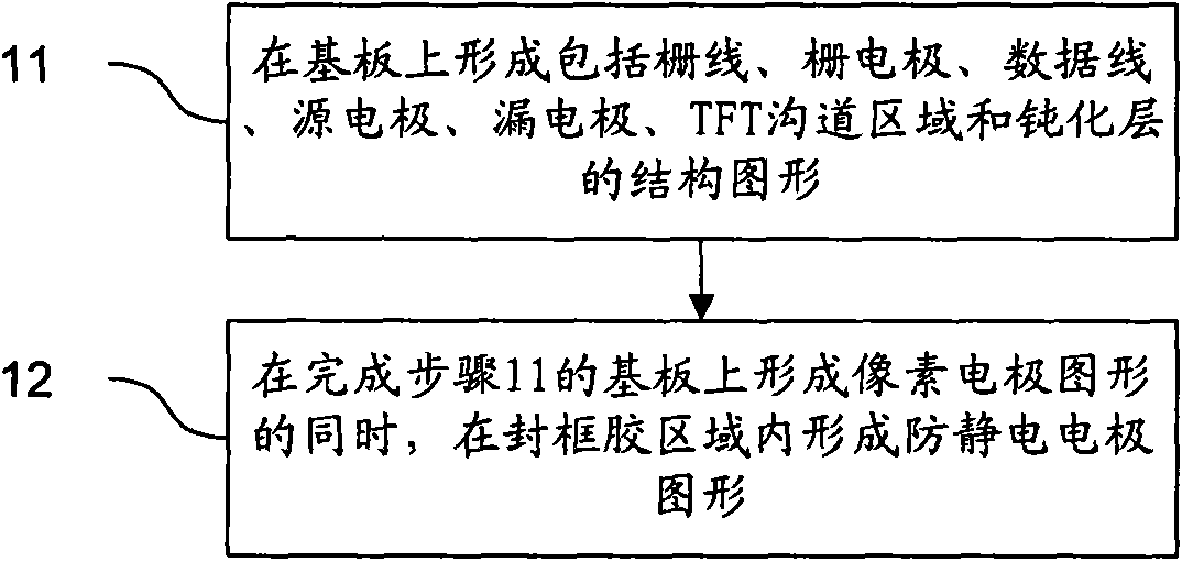
[0046] figure 1 It is a flow chart of the first embodiment of the manufacturing method of the liquid crystal display array substrate of the present invention, specifically including:

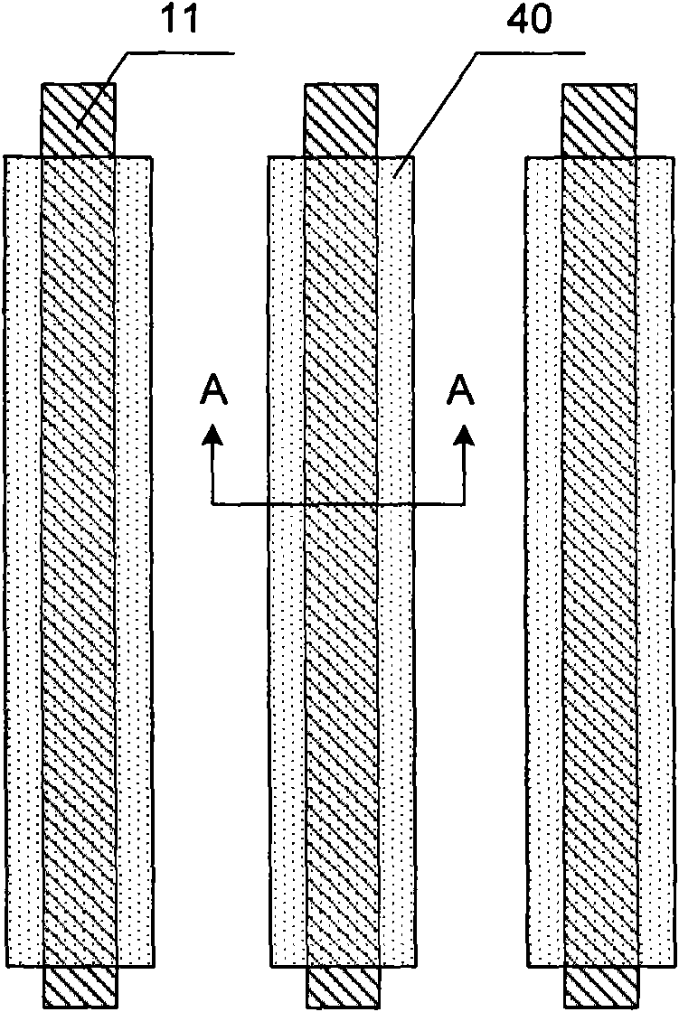
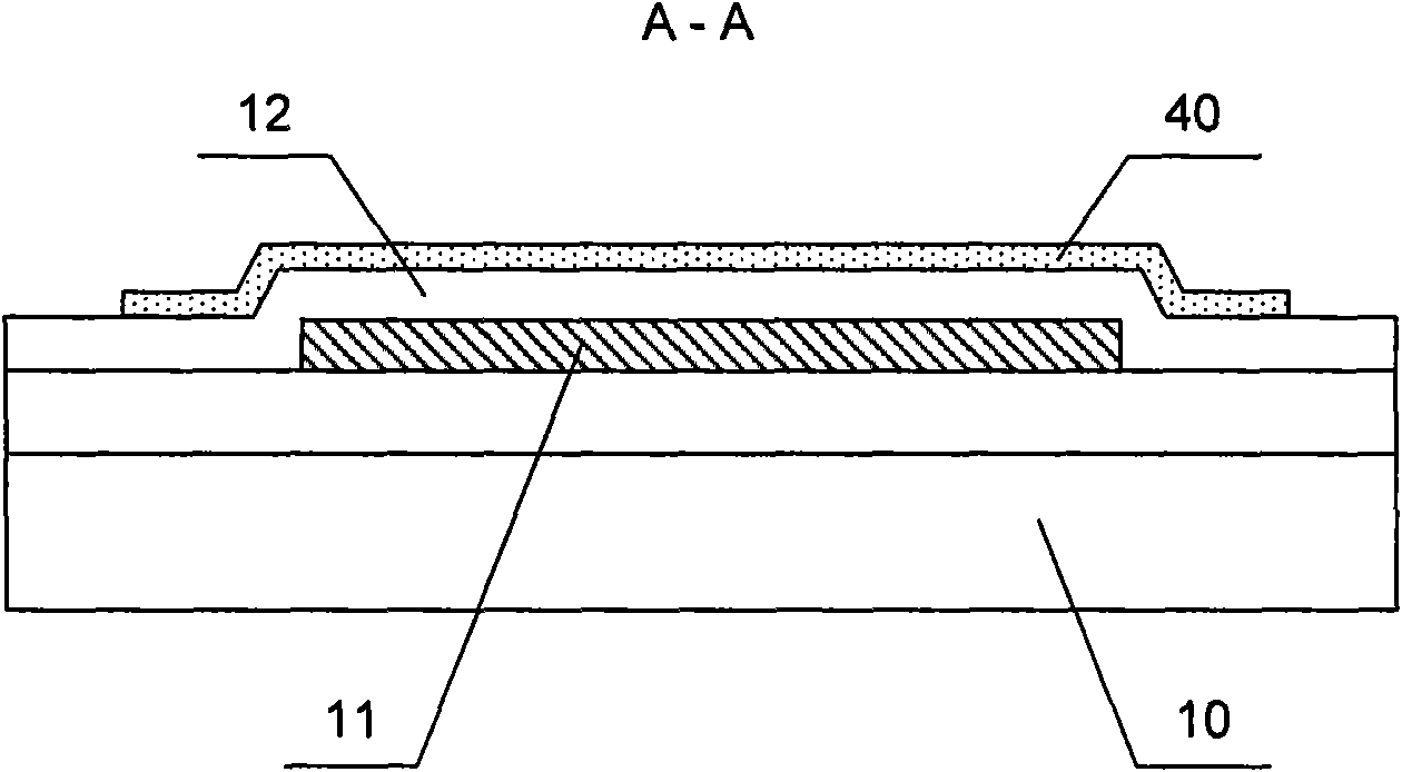
[0047] Step 11, forming a structural pattern including gate lines, gate electrodes, data lines, source electrodes, drain electrodes, TFT channel regions and passivation layers on the substrate;

[0048]Step 12: While forming the pixel electrode pattern on the substrate completed in step 11, an antistatic electrode pattern is formed in the sealant area.

[0049] This embodiment provides a method for manufacturing an array substrate of a liquid crystal display. An antistatic electrode is formed at the same time as the pattern of the pixel electrode is formed, and the antistatic electrode is located in the frame sealing area, which is the subsequent array substrate and color filter substrate. The area where the sealant is applied when the box is aligned, and the sealant contains gold balls. Afte...


PUM


Abstract

The invention relates to a liquid crystal display array substrate and a manufacturing method thereof. The manufacturing method comprises the following steps: forming a structural figure comprising a grid line, a gate electrode and an active layer on a substrate; forming a structural figure comprising a data wire, a source electrode, a drain electrode and a TFT channel area, wherein the two sides of the data wire are in a slope shape or a stepped shape for preventing the aggregation of static electricity; forming the figure of a passivation layer; and forming the figure of a pixel electrode, and forming the figure of an anti-static electrode simultaneously in a frame sealant area. The two sides of the data wire are in the slope shape or the stepped shape preventing the aggregation of the static electricity, thus electrostatic discharge possibly caused by the edges and corners of the data wire is dispersed effectively; and simultaneously, the anti-static electrode is formed in the framesealant area to reduce the density of the static electricity accumulated on the surface of a golden ball, so the electrostatic discharge between the data wire and the golden ball can be avoided, and the defect of imperfect bright line caused by a short circuit between the data wire and the golden ball can be effectively prevented.

Description

technical field [0001] The invention relates to a liquid crystal display and a manufacturing method thereof, in particular to a liquid crystal display array substrate and a manufacturing method thereof. Background technique [0002] The main structure of a liquid crystal display (Liquid Crystal Display, LCD) includes an array substrate and a color filter substrate that are boxed together and the liquid crystal is sandwiched between them. The array substrate is formed with gate lines that provide scanning signals, data lines that provide data signals, and A pixel electrode forming a pixel point, and a black matrix, a color resin, and a common electrode for providing a common voltage are formed on the color filter substrate. In the one-time sealing glue coating process of combining the array substrate and the color filter substrate together, in order to ensure the conduction between the common electrode of the array substrate and the common electrode of the color filter substr...

Claims


Application Information

Patent Timeline
IPC IPC(8): G02F1/1362H01L27/12H01L21/84G03F7/00
Inventor 邱海军王章涛闵泰烨
Owner BEIJING BOE OPTOELECTRONCIS TECH CO LTD
Why Eureka
Try Eureka