Manufacturing method of gallium nitride based LED with vertical structure

A light-emitting diode, gallium nitride-based technology, applied in the direction of electrical components, circuits, semiconductor devices, etc., can solve the problems of poor reliability and light efficiency reduction of vertical GaN-based light-emitting diodes, etc., achieve good thermal stability, avoid Poor thermal stability, effects of maintaining luminous efficiency and reliability

Active Publication Date: 2010-03-03
XIAMEN SANAN OPTOELECTRONICS TECH CO LTD
View PDF2 Cites 33 Cited by
  • Summary
  • Abstract
  • Description
  • Claims
  • Application Information

AI Technical Summary

Problems solved by technology

[0004] In order to solve the above-mentioned problem that the ohmic contact electrode on the GaN-based material on the nitrogen polar surface is susceptible to temperature cracking, which leads to the reduction of lig

Method used


Image

  • Manufacturing method of gallium nitride based LED with vertical structure
  • Manufacturing method of gallium nitride based LED with vertical structure
  • Manufacturing method of gallium nitride based LED with vertical structure

Examples


Embodiment Construction

[0030] The present invention will be further described below in conjunction with the accompanying drawings and embodiments.

[0031] A method for manufacturing a gallium nitride-based light-emitting diode with a vertical structure, the manufacturing steps of which are as follows:

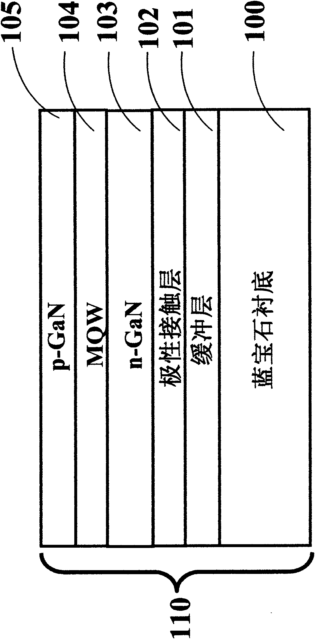
[0032] Such as Figure 1a As shown, making an epitaxial wafer 110 includes epitaxially growing a buffer layer 101, a polar contact layer 102, an n- GaN layer 103, multi-quantum well (MQW) active layer 104, and p-GaN layer 105, wherein the polar contact layer 102 is a nitrogen polar surface n-GaN, and the growth surface of n-GaN layer 103 is a gallium pole sex.

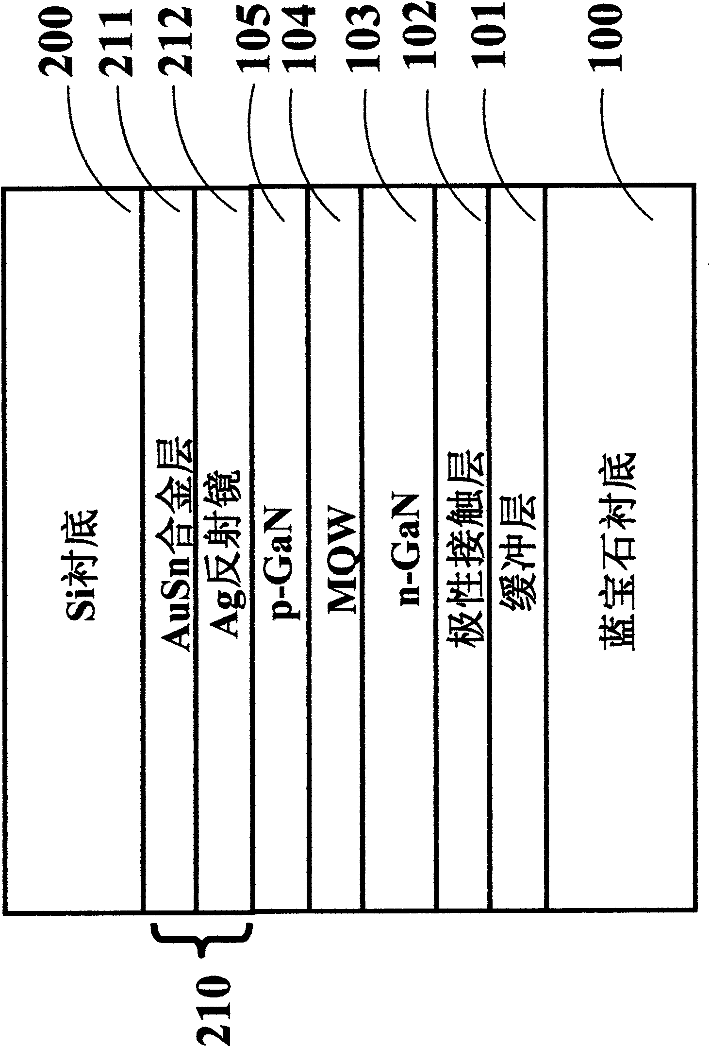
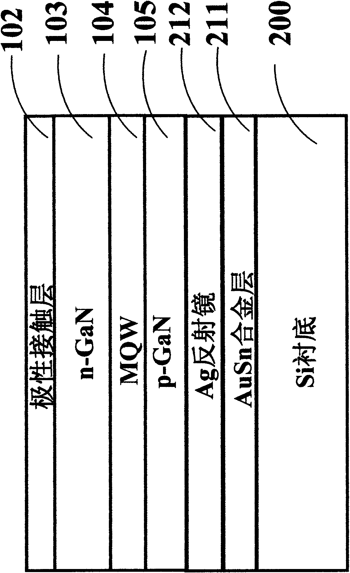
[0033] Such as Figure 1b As shown, a 100nm thick Ag mirror 211 is evaporated on the p-GaN layer 105, and the Ag mirror 211 not only plays a reflective role but also acts as an ohmic contact with the p-GaN layer 105; take a Si substrate 200 as Permanent substrate, on the Si substrate 200 evaporate a 2 micron thick AuSn (80: 20) alloy lay...


PUM


Abstract

The invention discloses a manufacturing method for a gallium nitride based LED with a vertical structure. During the manufacture of the gallium nitride based LED with the vertical structure, an n-typeGaN-based material is adopted as a polar contact extension layer which is in nitrogen polarity, and after a temporary growth substrate is removed, the surface of the polar contact extension layer isin gallium polarity; based on the base, an n-type ohm contact electrode, that is n-type ohm contact is formed on the n-type GaN-based material of a gallium polar surface, so the n-type ohm contact with good thermal stability can be obtained and the problem of poor thermal stability of ohm contact on the nitrogen polar surface is avoided; and in the LED with the vertical structure manufactured by the manufacturing process, the n-type ohm contact of which has better thermal stability, the working voltage is not changed along the change of outside temperature, therefore, the illumination efficiency and the reliability of the LED can be maintained.

Description

technical field [0001] The invention relates to a method for manufacturing a light-emitting diode, in particular to a method for manufacturing a gallium nitride-based light-emitting diode with a vertical structure. Background technique [0002] In recent years, in order to improve the luminous power and efficiency of gallium nitride (GaN)-based light-emitting diodes, a vertical structure chip technology based on substrate transfer has been developed. It is bonded to a semiconductor or metal substrate by wafer bonding technology or electroplating technology, and then the sapphire substrate is removed by laser lift-off method; or GaN-based luminescent material is epitaxially deposited on SiC or Si substrate, and then the luminescent material layer is passed through the crystal. The round bonding technology or electroplating technology is bonded to the semiconductor or metal substrate, and then the SiC or Si substrate is removed by chemical etching. In this way, on the one han...

Claims


Application Information

Patent Timeline
IPC IPC(8): H01L33/00
Inventor 潘群峰林雪娇吴志强
Owner XIAMEN SANAN OPTOELECTRONICS TECH CO LTD
Why Eureka
Try Eureka