Apparatus and method for atomic layer deposition

A technology of atomic layer deposition and deposition cycle, which is applied in the field of atomic layer deposition devices and methods, can solve problems such as copper diffusion and damage to device integrity, and achieve the effect of increasing flux

Inactive Publication Date: 2010-03-03
LAM RES CORP
View PDF0 Cites 4 Cited by
  • Summary
  • Abstract
  • Description
  • Claims
  • Application Information

AI Technical Summary

Problems solved by technology

One problem with using copper is that it diffuses into silicon, silicon dioxide, and other dielectric materials, which can compromise the integrity of the device

Method used


Image

  • Apparatus and method for atomic layer deposition
  • Apparatus and method for atomic layer deposition
  • Apparatus and method for atomic layer deposition

Examples


Embodiment Construction

[0034] Some exemplary embodiments of ALD apparatus and methods using proximity heads are provided. The proximity head ALD apparatus and method improves ALD processing throughput and allows pre-treatment and post-treatment of ALD deposition in the same apparatus. It should be understood that the present invention can be implemented in various ways, including process, method, apparatus or system. Some innovative embodiments of the present invention are described below. It will be apparent to one skilled in the art that the present invention may be practiced without some or all of the specific details set forth herein.

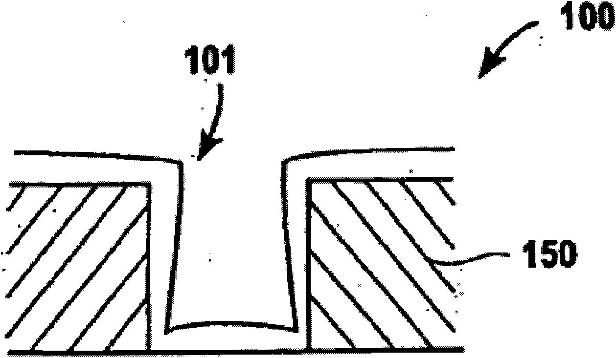
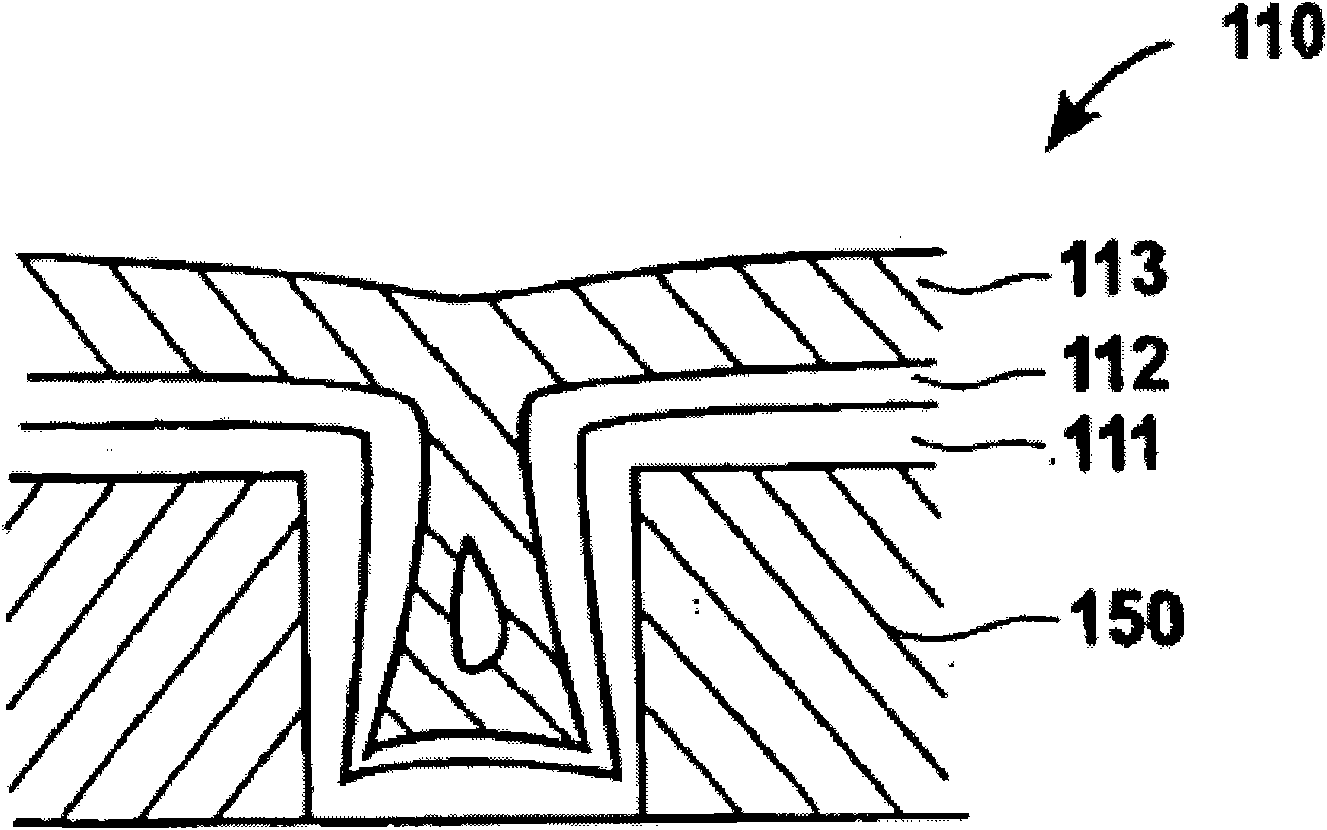
[0035] like Figure 1A As shown, it is known that the barrier protrusion 101 near the top of the interconnect structure 100 produced by a conventional physical vapor deposition (PVD) process can lead to metal interconnection due to poor step coverage during copper void filling. Copper voids in lines or vias. like Figure 1A As shown, limited deposition of barr...


PUM

PropertyMeasurementUnit
thicknessaaaaaaaaaa
thicknessaaaaaaaaaa

Abstract

The embodiments provide apparatus and methods of depositing conformal thin film on interconnect structures by providing processes and systems using an atomic layer deposition (ALD). More specifically,each of the ALD systems includes a proximity head (430) that has a small reaction volume right above an active process region of the substrate surface (410). The proximity head small amount of reactants and purging gas to be distributed and pumped away from the small reaction volume between the proximity head and the substrate in relatively short periods, which increases the through-put. In an exemplary embodiment, a proximity head for dispensing reactants and purging gas to deposit a thin film by atomic layer deposition (ALD) is provided. The proximity head is configured to sequentially dispensing a reactant gas (445, 443) and a purging gas (441) to deposit a thin ALD film under the proximity head. The proximity head covers an active process region of a substrate surface. The proximity head also includes at least one vacuum channel (465) to pull excess reactant gas, purging gas, or deposition byproducts from a reaction volume (450) between a surface of the proximity head facing the substrate and the substrate. The proximity includes a plurality of sides, each side being configured to dispense either a reactant gas or a purging gas on the substrate surface underneath the proximityhead. Each side has at least one vacuum channel.

Description

Background technique [0001] In the fabrication of semiconductor devices, such as integrated circuits, memory cells, etc., a series of fabrication operations are performed to define features on a semiconductor wafer. The semiconductor wafer includes integrated circuit devices in the form of a multi-level structure defined on a silicon substrate. At the substrate level, transistor devices are formed with diffusion regions. At subsequent levels, interconnect metallization lines are patterned and electrically connected to the transistor devices to define the desired integrated circuit device. Also, the dielectric material insulates the patterned conductive layer from other conductive layers. [0002] Reliable production of sub-micron and smaller features is one of the key technologies for next-generation very large-scale integration (VLSI) and ultra-large-scale integration (ULSI) of semiconductor devices. However, in VLSI and VLSI technologies, the ever-shrinking size of interc...

Claims


Application Information

Patent Timeline
Patent Type & Authority Applications(China)
IPC IPC(8): H01L21/20H01L21/44C23C16/00
CPCH01L21/76843H01L21/28562C23C16/45551C23C16/00H01L21/205H01L21/44C23C16/45517C23C16/54
Inventor 衡石·亚历山大·尹约翰·M·博迪米哈伊尔·科罗利克耶兹迪·多尔迪弗里茨·C·雷德克
Owner LAM RES CORP
Why Eureka
Try Eureka