

Manufacturing method of thin film transistor array substrate
A technology of thin film transistors and manufacturing methods, which is applied in the field of liquid crystal display manufacturing, can solve the problems of lowering manufacturing costs and high cost of large-size photomasks, and achieve the effect of saving photomask costs
- Summary
- Abstract
- Description
- Claims
- Application Information
AI Technical Summary
Problems solved by technology
Method used
Image

Examples
Embodiment Construction
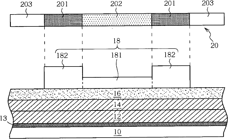
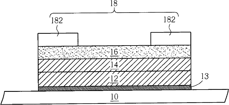
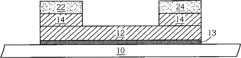
[0009] Please refer to Figure 1 to Figure 9 , which is a schematic diagram of the product structure corresponding to each step of the manufacturing method of the thin film transistor array substrate according to a preferred embodiment of the present invention. First please refer to figure 1 , provide a substrate 10, the upper surface of the substrate 10 is sequentially provided with a semiconductor layer 12, an ohmic contact layer 14 and a first metal layer 16, wherein the substrate 10 can be a glass substrate, a plastic substrate or a flexible substrate, semiconductor The layer 12 and the ohmic contact layer 14 comprise amorphous silicon or other semiconductor materials, and the ohmic contact layer 14 is an optional layer, which can be a heavily doped amorphous silicon layer; the first metal layer 16 can be made of metal, such as: Aluminum, molybdenum, titanium, chromium, copper or the metal oxide, such as titanium oxide, or the alloy of the metal or other conductive materi...
PUM
 Abstract
Description
Claims
Application Information