

Bit line leakage current compensation circuit for sub-threshold memory cell array
A memory cell array and compensation circuit technology, applied in information storage, static memory, digital memory information, etc., can solve the problems that the performance is easily affected by process deviation, the bit line swing is small in the read cycle, and the area loss is large. Achieve the effects of simple timing control signal, enhanced off current, and reduced area consumption
- Summary
- Abstract
- Description
- Claims
- Application Information
AI Technical Summary
Problems solved by technology
Method used
Image

Examples
Embodiment Construction
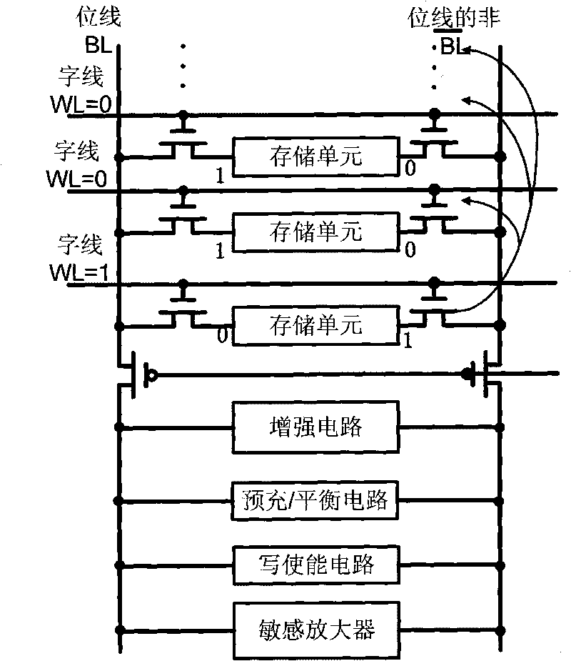
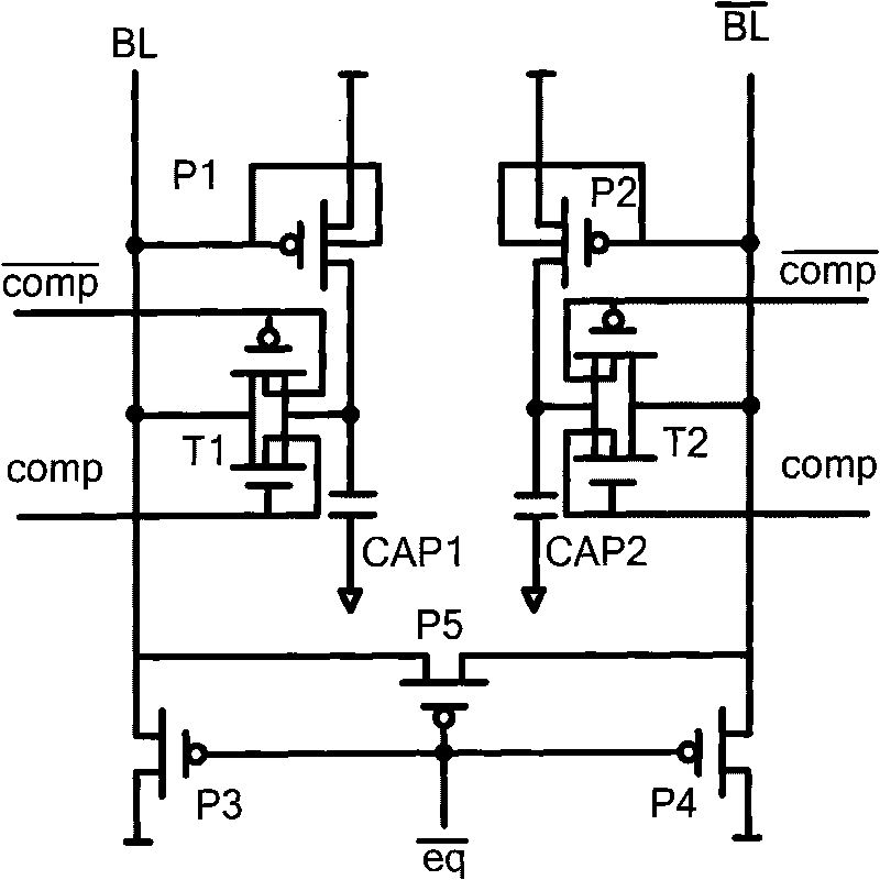
[0020] refer to figure 2 According to the present invention, a bit line leakage current compensation circuit of a sub-threshold memory cell array is composed of a first compensation transistor P1, a second compensation transistor P2, a first pre-charge balance transistor P3, a second pre-charge balance transistor P4, and a third pre-charge balance transistor. The charging and balancing transistor P5, the first shielding transmission gate T1, the second shielding transmission gate T2, and the first logic storage capacitor CAP1 and the second logic storage capacitor CAP2 are composed of the source end of the first compensation transistor P1 and the second compensation transistor P2 The source terminal is connected to the power supply voltage, the gate terminal of the first compensation transistor P1 is connected to the input terminal of the first shielded transmission gate T1 and serves as the bit line terminal of the memory cell array, and the gate terminal of the second compen...
PUM
 Abstract
Description
Claims
Application Information