AlGaN/GaN insulated gate high electron mobility transistor (HEMT) and manufacturing method thereof

A high electron mobility and transistor technology, applied in the field of microelectronics, can solve the problems of adding additional processes, device characteristic degradation, and low device yield, so as to improve reliability and stability, high device yield, and improve frequency characteristics Effect

Active Publication Date: 2010-05-19
XIAN CETC XIDIAN UNIV RADAR TECH COLLABORATIVE INNOVATION INST CO LTD
View PDF0 Cites 27 Cited by
  • Summary
  • Abstract
  • Description
  • Claims
  • Application Information

AI Technical Summary

Problems solved by technology

[0005] In summary, the current existing technology cannot effectively reduce the source-drain distance and improve the frequency characteristics of the device. In addition, it also has the following problems: first, it complicates the device manufacturing steps and add

Method used


Image

  • AlGaN/GaN insulated gate high electron mobility transistor (HEMT) and manufacturing method thereof
  • AlGaN/GaN insulated gate high electron mobility transistor (HEMT) and manufacturing method thereof
  • AlGaN/GaN insulated gate high electron mobility transistor (HEMT) and manufacturing method thereof

Examples


Embodiment 1

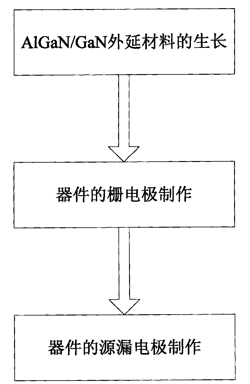
[0030] Embodiment 1, the making of device of the present invention, comprises the following steps:

[0031] Step 1. Epitaxial material growth.

[0032] refer to figure 1 and figure 2 , the specific implementation of this step is as follows:

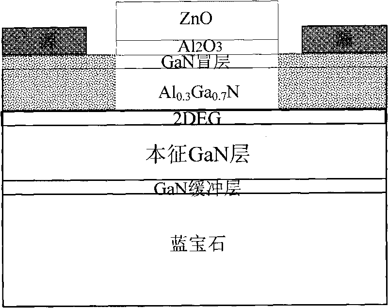
[0033] (101) On the sapphire substrate substrate, utilize the MOCVD process to grow a GaN buffer layer;

[0034] (102) growing an intrinsic GaN layer on the GaN buffer layer;

[0035] (103) On the intrinsic GaN layer, a 24nm thick Al 0.3 Ga 0.7 N layer;

[0036] (104) in Al 0.3 Ga 0.7 On the N layer, a 2nm thick GaN capping layer is grown.

[0037] Step 2. Make the gate electrode.

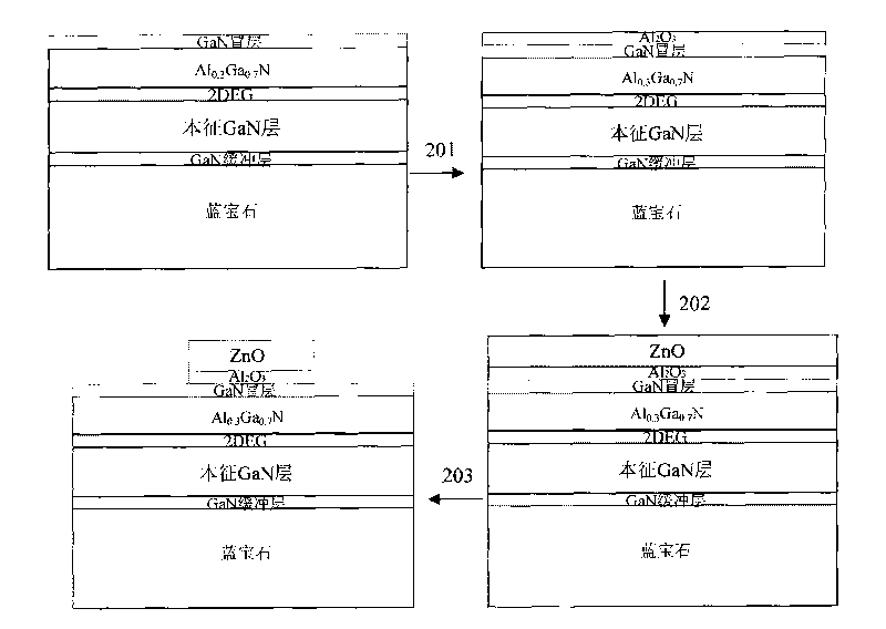
[0038] refer to figure 1 and image 3 , the specific implementation of this step is as follows:

[0039] (201) Deposit Al on the surface of the sample by atomic layer deposition (ALD) 2 o 3 The dielectric layer is deposited with a thickness of 5nm and a temperature of 300°C.

[0040] Firstly, boil and wash the sample in stripping solution for 20...

Embodiment 2

[0054] Embodiment 2, the making of device of the present invention, comprises the following steps:

[0055] Step 1. Epitaxial material growth.

[0056] refer to figure 1 and figure 2 , the specific implementation of this step is as follows:

[0057] (101) On the sapphire substrate substrate, utilize the MOCVD process to grow a GaN buffer layer;

[0058] (102) growing an intrinsic GaN layer on the GaN buffer layer;

[0059] (103) On the intrinsic GaN layer, a 24nm thick Al 0.3 Ga 0.7 N layer;

[0060] (104) in Al 0.3 Ga 0.7 On the N layer, a 2nm thick GaN capping layer is grown.

[0061] Step 2. Make the gate electrode.

[0062] refer to figure 1 and image 3 , the specific implementation of this step is as follows:

[0063] (201) Deposit Al on the surface of the sample by atomic layer deposition (ALD) 2 o 3 The dielectric layer is deposited with a thickness of 7nm and a temperature of 300°C.

[0064] Firstly, boil and wash the sample in stripping solution for ...

Embodiment 3

[0078] Embodiment 3, the making of device of the present invention, comprises the following steps:

[0079] Step 1. Epitaxial material growth.

[0080] refer to figure 1 and figure 2 , the specific implementation of this step is as follows:

[0081] (101) On the sapphire substrate substrate, utilize the MOCVD process to grow a GaN buffer layer;

[0082] (102) growing an intrinsic GaN layer on the GaN buffer layer;

[0083] (103) On the intrinsic GaN layer, a 24nm thick Al 0.3 Ga 0.7 N layer;

[0084] (104) in Al 0.3 Ga 0.7 On the N layer, a 2nm thick GaN capping layer is grown.

[0085] Step 2. Make the gate electrode.

[0086] refer to figure 1 and image 3 , the specific implementation of this step is as follows:

[0087] (201) Deposit Al on the surface of the sample by atomic layer deposition (ALD) 2 o 3 The dielectric layer is deposited with a thickness of 10nm and a temperature of 300°C.

[0088] Firstly, boil and wash the sample in stripping solution for 2...


PUM


Abstract

The invention discloses an AlGaN/GaN insulated gate high electron mobility transistor (HEMT) device and a manufacturing method thereof, relating to the field of microelectronic technique and mainly solving the problems of low frequency and poor radiation resistance of the device. The device comprises a GaN buffer layer, an intrinsic GaN layer, an AlO.3GaO.7N layer, a GaN coating layer, a gate oxide layer, a gate electrode, a source electrode and a drain electrode, wherein Al2O3 is used as the gate oxide layer, and transparent ZnO is used as the gate electrode. The Al element is doped in the ZnO gate electrode, and the length of the ZnO gate electrode is equal to the distance between the source electrode and the drain electrode. The manufacturing method of the device sequentially comprises the steps of: firstly, carrying out epitaxial material growth, then manufacturing the Al2O3 gate oxide layer and the ZnO gate electrode, and finally, manufacturing the source electrode and the drain electrode at two sides of the ZnO gate electrode by using a self-aligned method. The device has the advantages of good frequency characteristics, good radiation resistance, simple processes, good repeatability and high reliability, thereby being used as an electronic component in a high frequency circuit or a high speed circuit.

Description

technical field [0001] The invention belongs to the technical field of microelectronics and relates to semiconductor devices, specifically a structure and a realization method of a short-channel AlGaN / GaN insulating gate high electron mobility transistor using transparent material ZnO as a gate and source-drain self-alignment technology , used as high-speed devices and high-frequency devices. Background technique [0002] Compared with the parameters of other semiconductor materials, GaN material has obvious advantages. Its forbidden band width is the widest, its saturation electron velocity is also better than other semiconductor materials, and it has a large breakdown field strength and high thermal conductivity. The characteristics of charge carrier velocity field are the basis of device operation. High saturation velocity leads to large current and high frequency. High breakdown field strength is crucial for high-power applications of devices. At the same time, due to th...

Claims


Application Information

Patent Timeline
IPC IPC(8): H01L29/778H01L29/43H01L29/08H01L21/335H01L21/285
Inventor 马晓华郝跃曹艳荣王冲高海霞杨凌
Owner XIAN CETC XIDIAN UNIV RADAR TECH COLLABORATIVE INNOVATION INST CO LTD
Why Eureka
Try Eureka