

Semiconductor device and method for fabricating the same
A manufacturing method and semiconductor technology, which are applied in semiconductor/solid-state device manufacturing, semiconductor devices, electrical components, etc., can solve the problems of difficulty in obtaining threshold voltage and difficulty in controlling the impurity concentration in the channel region, and achieve the effect of easy control.
- Summary
- Abstract
- Description
- Claims
- Application Information
AI Technical Summary
Problems solved by technology
Method used
Image

Examples
no. 1 Embodiment
[0055] -Structure of semiconductor device-
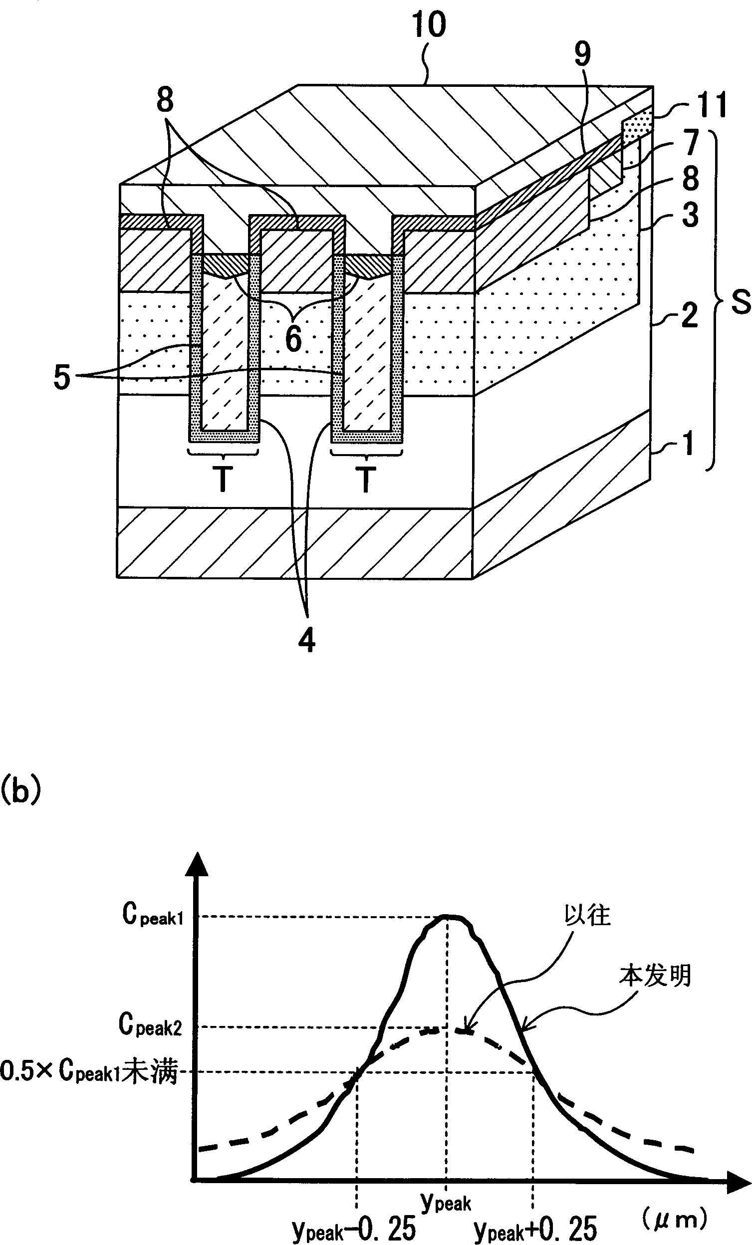
[0056] Fig. 1(a) is a perspective view showing the structure of a semiconductor device having a trench gate structure according to the first embodiment of the present invention, and Fig. 1(b) is a perspective view showing the The second conductivity type impurity concentration profile in the vertical direction in the semiconductor device. In addition, in FIG. 1( a ), illustration of the barrier metal layer provided on the lower side of the contact electrode 10 is omitted for easier viewing.
[0057] As shown in Figure 1(a), the semiconductor device of this embodiment includes: a high-concentration N-type drain region 1 formed at least in a region near the back surface of a semiconductor substrate S made of silicon; a low-concentration N-type drain region 2, set on the high-concentration N-type drain region 1 in the semiconductor substrate S; the P-type substrate region 3, selectively set on the low-concentration N-type drain region...
no. 2 Embodiment
[0095] -Structure of semiconductor device-
[0096] The semiconductor device having the trench gate structure according to the second embodiment of the present invention has the structure shown in FIG. 1( a ) as in the first embodiment.
[0097] The difference between the present embodiment and the first embodiment lies in the second conductivity type impurity concentration distribution along the vertical direction in the semiconductor device shown in FIG. 1( a ).
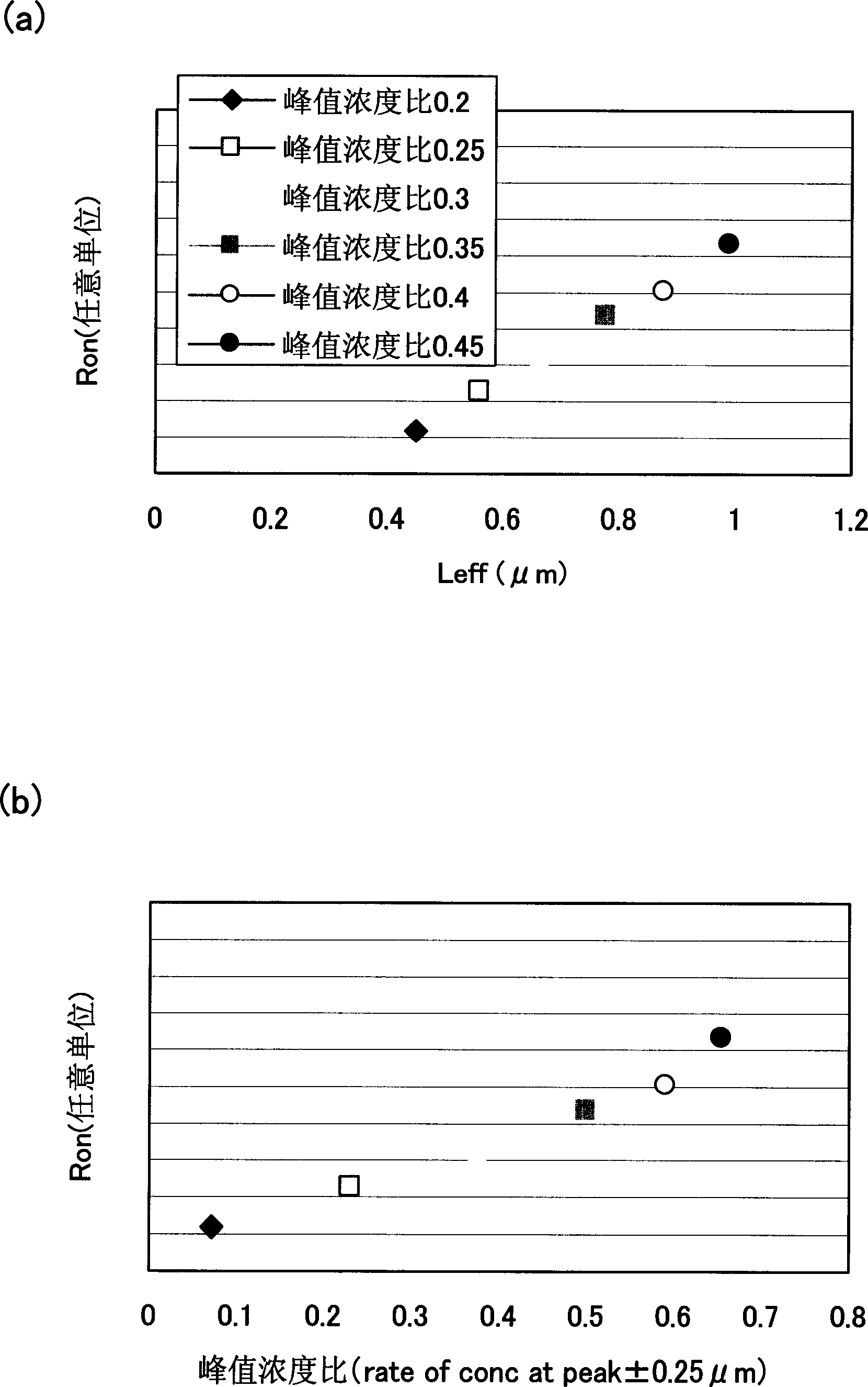
[0098] Figure 7 The concentration distribution in the depth direction of the second conductivity type (P type) impurity that determines the threshold voltage (Vt) in the P type substrate region 3 sandwiched by adjacent trenches T is shown.
[0099] Such as Figure 7 As shown, in this embodiment, the second conductivity type impurity is introduced into the semiconductor substrate S by two ion implantations to form a distribution with two peaks, thereby determining the threshold voltage (vt).
[0100] Like this, ...
no. 1 Embodiment 1
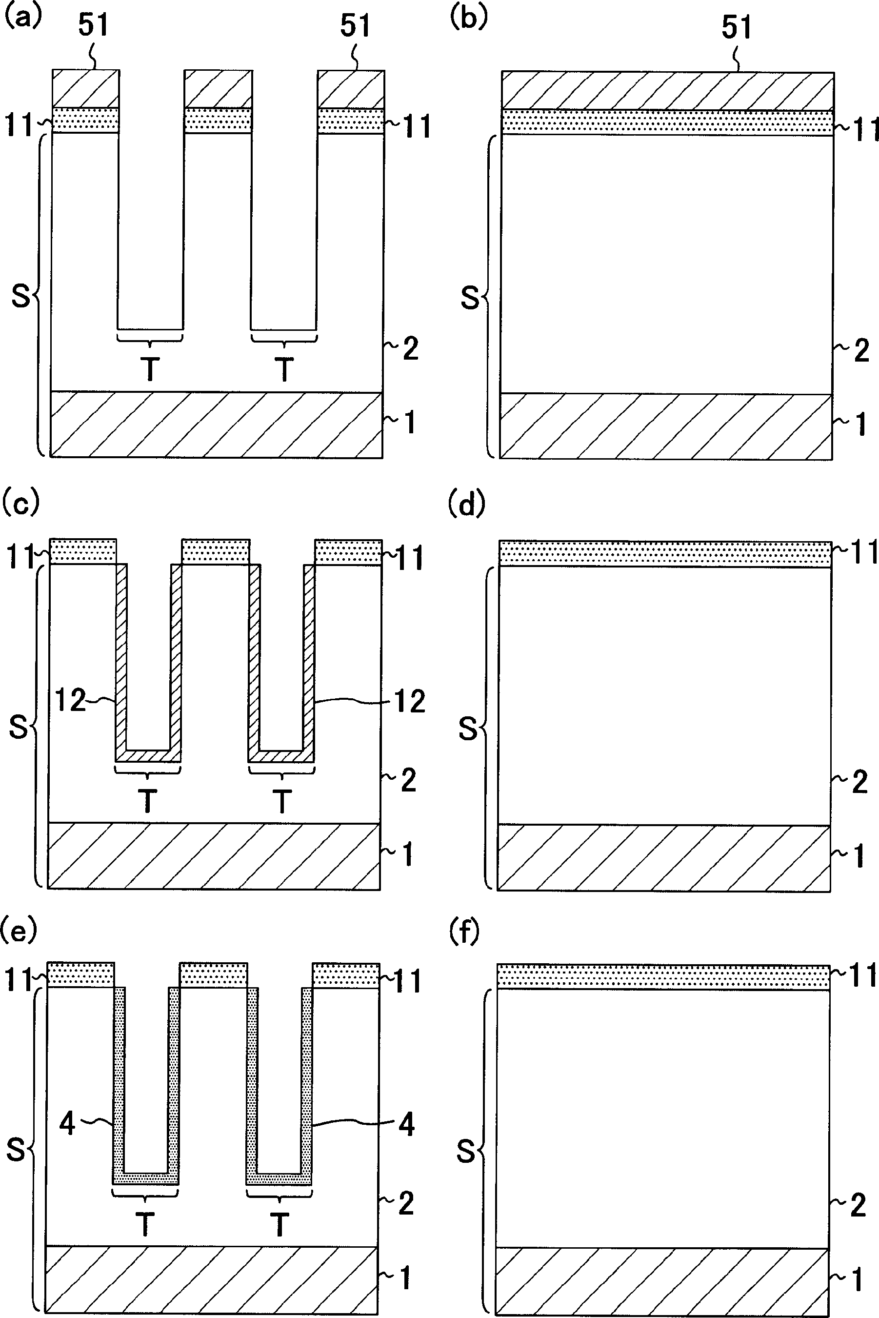
[0105] The differences between this embodiment and the first embodiment are: Figure 4 (c), Figure 4 The detailed process of the ion implantation process shown in (d). Specifically, in this embodiment, a photoresist mask 52 having an opening in a predetermined region including a source region and a high-concentration P-type substrate region to be formed in a later step is formed on the polysilicon film 5A. Then, by ion implantation using the photoresist mask 52, P-type impurities are introduced into the upper part of the low-concentration N-type drain region 2 through the polysilicon film 5A and the protective insulating film 11. When the P-type substrate region 3 is about 1 μm, the ion implantation of the P-type impurity is performed twice. Here, the conditions for the first ion implantation are that the implantation energy is, for example, 600-700 keV, and the doping quality is, for example, 6.0×10 12 ions / cm 2 , the condition of the second ion implantation is that the ...
PUM
 Abstract
Description
Claims
Application Information