LDMOS device with transverse diffusing buried layer below grid

A horizontal and device technology, applied in the direction of semiconductor devices, semiconductor/solid-state device manufacturing, electrical components, etc., can solve the problems of increasing nonlinear capacitance, achieve the effects of reducing various nonlinear capacitances, improving surge resistance, and improving performance

Active Publication Date: 2010-06-02
INNOGRATION SUZHOU +2
View PDF0 Cites 11 Cited by
  • Summary
  • Abstract
  • Description
  • Claims
  • Application Information

AI Technical Summary

Problems solved by technology

However, the increased dose of doping ions implanted in the channel region often leads to an increase in the nonlinear capacitance of the device.
Therefore, th

Method used


Image

  • LDMOS device with transverse diffusing buried layer below grid
  • LDMOS device with transverse diffusing buried layer below grid
  • LDMOS device with transverse diffusing buried layer below grid

Examples


Embodiment

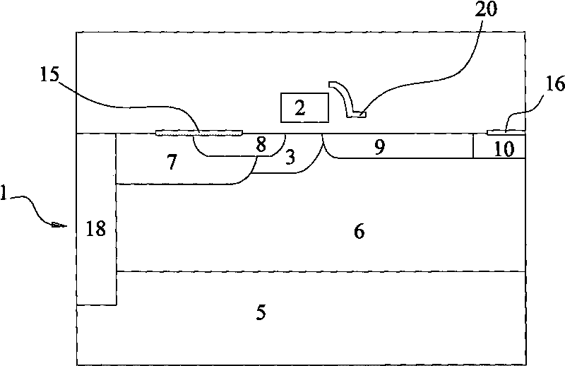
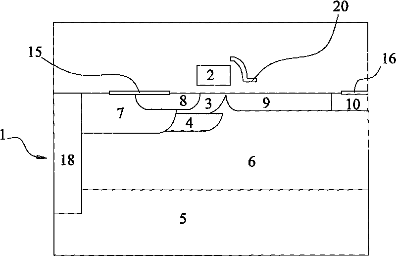
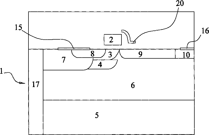
[0023] Example: such as figure 2 and image 3 As shown, an LDMOS device with a source-drain breakdown voltage between 60V-120V and a laterally diffused buried layer under the gate includes a semiconductor body 1 and a gate 2 on the semiconductor body 1, and the semiconductor body 1 is connected to the gate 2 A doped channel region 3 of the first conductivity type is provided below, and a lateral diffusion buried layer 4 of the first conductivity type is provided below the doped channel region 3 of the first conductivity type. The semiconductor body 1 further includes a heavily doped substrate 5 of the first conductivity type, an epitaxial layer 6 of the first conductivity type on the heavily doped substrate 5 of the first conductivity type, and the doped channel region 3 of the first conductivity type Located on the epitaxial layer 6 of the first conductivity type, one side of the doped channel region 3 of the first conductivity type is adjacent to a heavily doped source reg...


PUM


Abstract

The invention discloses an LDMOS device with a transverse diffusing buried layer below a grid, comprising a semiconductor body and the grid positioned on the semiconductor body. A first conduction type doping channel region is arranged on the semiconductor body and below the grid; and a first conduction type transverse diffusing buried layer is arranged below the first conduction type doping channel region. The invention can properly reduce the use level of doping ions injected to the first conduction type doping channel region under the precondition of effectively inhibiting the short channel effect of the LDMOS device, thereby reducing the nonlinear capacitors of the LDMOS device so that the radio frequency power and the performance of the LDMOS device are further improved.

Description

technical field [0001] The invention relates to an LDMOS device with a lateral diffusion buried layer under the gate Background technique [0002] In RF power LDMOS devices, in order to improve the output power, power gain and linearity of the device, it is required to suppress the device threshold voltage caused by the short channel effect of the device as much as possible while meeting the requirements of the drain-source breakdown voltage BVdss Vth and drain-source output current Ids drift with the drain-source voltage Vds, while minimizing various nonlinear capacitances of the device such as gate-source capacitance Cgs, gate-drain capacitance Cgd and drain-source capacitance Cds. The short channel effect of the device is usually suppressed by increasing the dose of dopant ions implanted into the channel region under the gate of the LDMOS device and adjusting the lateral diffusion conditions of this ion implantation layer. However, the increased dose of doping ions impla...

Claims


Application Information

Patent Timeline
IPC IPC(8): H01L29/78H01L21/336H01L21/266
CPCH01L29/66659H01L29/402H01L29/4175H01L29/7835H01L29/105H01L29/1083
Inventor 陈强马强
Owner INNOGRATION SUZHOU
Why Eureka
Try Eureka