LDMOS device with transverse diffusing buried layer below grid
A horizontal and device technology, applied in the direction of semiconductor devices, semiconductor/solid-state device manufacturing, electrical components, etc., can solve the problem of increasing nonlinear capacitance, achieve the effects of reducing various nonlinear capacitances, improving performance, and improving surge resistance
- Summary
- Abstract
- Description
- Claims
- Application Information
AI Technical Summary
Problems solved by technology
Method used
Image
Examples
Embodiment
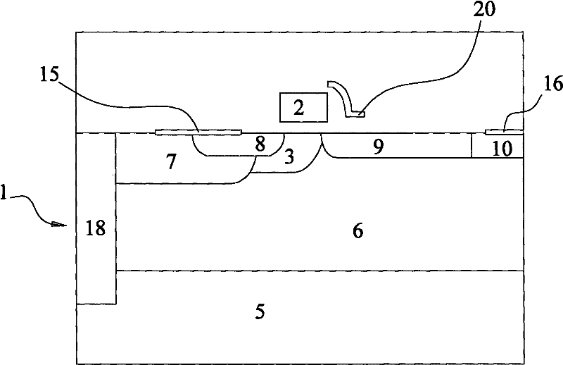
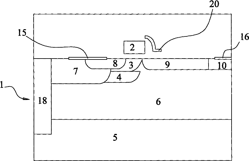
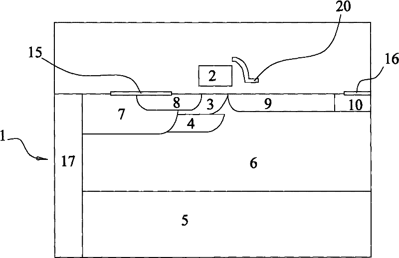
[0023] Example: such as figure 2 and image 3 As shown, an LDMOS device with a source-drain breakdown voltage between 60V-120V and a laterally diffused buried layer under the gate includes a semiconductor body 1 and a gate 2 on the semiconductor body 1, and the semiconductor body 1 is connected to the gate 2 A doped channel region 3 of the first conductivity type is provided below, and a lateral diffusion buried layer 4 of the first conductivity type is provided below the doped channel region 3 of the first conductivity type. The semiconductor body 1 further includes a heavily doped substrate 5 of the first conductivity type, an epitaxial layer 6 of the first conductivity type on the heavily doped substrate 5 of the first conductivity type, and the doped channel region 3 of the first conductivity type Located on the epitaxial layer 6 of the first conductivity type, one side of the doped channel region 3 of the first conductivity type is adjacent to a heavily doped source reg...
PUM
 Abstract
Description
Claims
Application Information
 - R&D
- Intellectual Property
- Life Sciences
- Materials
- Tech Scout
- Unparalleled Data Quality
- Higher Quality Content
- 60% Fewer Hallucinations
Browse by: Latest US Patents, China's latest patents, Technical Efficacy Thesaurus, Application Domain, Technology Topic, Popular Technical Reports.
© 2025 PatSnap. All rights reserved.Legal|Privacy policy|Modern Slavery Act Transparency Statement|Sitemap|About US| Contact US: help@patsnap.com


