Method for drilling holes on printed circuit board

A printed circuit board, laser drilling technology, applied in laser welding equipment, welding equipment, metal processing equipment and other directions, can solve the problems of high machine cost, low carbon dioxide laser absorption rate, slow processing speed, etc., to achieve cost saving. Effect

Inactive Publication Date: 2010-06-09
COMPEQ MFG
View PDF0 Cites 16 Cited by
  • Summary
  • Abstract
  • Description
  • Claims
  • Application Information

AI Technical Summary

Problems solved by technology

[0004] At present, the drilling method on the printed circuit board mainly uses the laser drilling method with fast processing speed and small aperture, and the type of laser used is carbon dioxide (CO 2 ) laser and garnet (ND:YAG) laser, etc. Among them, carbon dioxide laser is used. Due to the high brightness of the copper foil surface, the absorption rate of carbon dioxide laser is quite low, so the copper foil at the position to be drilled must be pre-drilled. Removal, that is to form the so-called copper window (Conformal Mask), and then use carbon dioxide laser to break through the substrate to achieve the purpose of drilling. However, an additional image transfer process must be performed to make the copper window, and once the position of the copper window deviates, It will lead to the disadvantage of deviation of the drilling position on the substrate, and the use of garnet laser, because of its strong energy, can directly penetrate the copper foil and the substrate to complete the purpose of drilling without forming a copper window, while the garnet laser The laser drilling machine has the disadvantages that the processing speed is slower than that of the carbon dioxide laser drilling machine and the cost of the machine is expensive

Method used


Image

  • Method for drilling holes on printed circuit board
  • Method for drilling holes on printed circuit board
  • Method for drilling holes on printed circuit board

Examples


Embodiment Construction

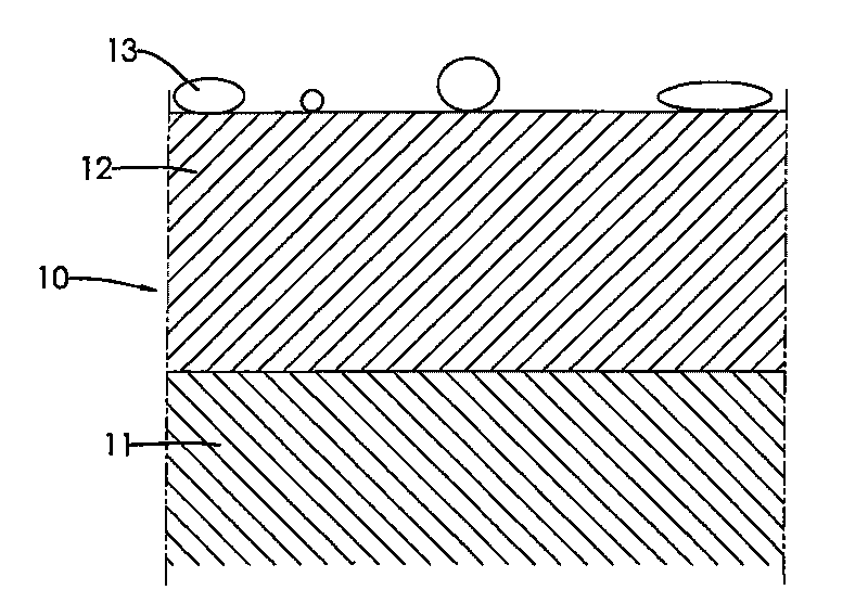
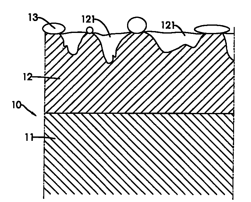
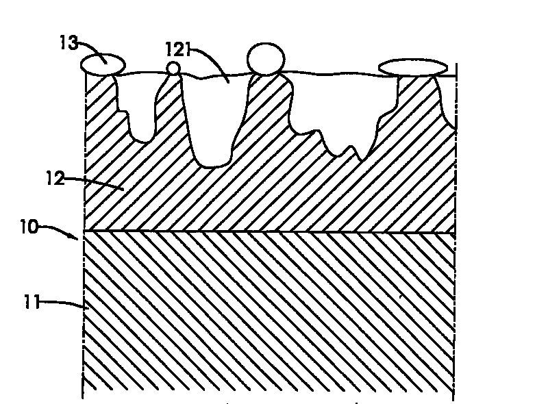
[0023] See figure 1 As shown, the present invention firstly provides a substrate 11 covered with copper foil 12 on one side of the board, the substrate 11 is made of insulating material, the insulating material can be resin, and the substrate 11 is on at least one side of the board Covered with copper foil 12, the thickness of the copper foil 12 can be between 12 and 18 μm, and then place the substrate 11 in an acid and alkali solution to remove oxides and grease on the surface of the copper foil 12, and then use a The cleaning solution is neutralized and cleaned. After cleaning, the copper foil 12 is chemically etched using an etching solution, which contains organic matter 13, sulfuric acid (H 2 SO 4 ), hydrogen peroxide (H 2 o 2 ) and an aqueous solution of copper ions, wherein sulfuric acid and hydrogen peroxide can corrode the copper foil, and their weight percentages can be 7 and 1.2 respectively, and the organic matter 13 can be uniformly dispersed and adsorbed on th...


PUM

PropertyMeasurementUnit
thicknessaaaaaaaaaa

Abstract

The invention relates to a method for drilling holes on a printed circuit board, comprising the following steps: providing the printed circuit board which comprises a substrate covered by a copper foil which has the thickness of 12-18 Mum on at least one side surface; washing the surface of the copper foil with acid and alkaline, neutralizing the acid and alkaline and cleaning the acid and alkaline; chemically etching the copper foil with etching solution which contains organic matter, sulfuric acid (H2SO4), hydrogen peroxide (H2O2) and copper ion to form a plurality of micro holes on the surface of the copper foil, wherein the organic matter can be uniformly dispersed and adsorbed on the surface of the copper foil, and the H2SO4 and H2O2 can etch the position where no organic matter is adsorbed; irradiating the position where holes to be drilled on the printed circuit board with the carbon dioxide laser and breaking down the copper foil and the substrate to finish drilling holes on the printed circuit board.

Description

technical field [0001] The invention relates to a drilling method for a printed circuit board, in particular to a method in which the copper foil is chemically etched first, and then the copper foil and the substrate are penetrated by a laser to complete the drilling. Background technique [0002] The printed circuit board mainly uses an insulating material as the substrate, and the circuit formed by the conductive material is arranged on the substrate, which can be used for mounting electronic components, and the electrical connection between the electronic components is provided by the circuit. The method of forming the circuit is mainly because the substrate is covered with a copper foil, and then the designed circuit is formed by etching. [0003] With the demand for high performance and high density, printed circuit boards are gradually developing towards multilayers, and in order to form electrical connections between layers, through holes are formed on the printed cir...

Claims


Application Information

Patent Timeline
Patent Type & Authority Applications(China)
IPC IPC(8): B23K26/38B23K26/382
Inventor 江衍青纪大佣黄仁钦
Owner COMPEQ MFG
Why Eureka
Try Eureka