
Method for forming flash memory grid electrode and flash memory

A memory gate and flash technology, applied in the direction of electric solid-state devices, semiconductor devices, transistors, etc., can solve the problem of reducing the electrical performance of the control gate, and achieve the effect of preventing the decline of electrical performance and eliminating sags

Active Publication Date: 2011-10-05
SEMICON MFG INT (SHANGHAI) CORP
View PDF1 Cites 0 Cited by
  • Summary
  • Abstract
  • Description
  • Claims
  • Application Information

AI Technical Summary

Problems solved by technology

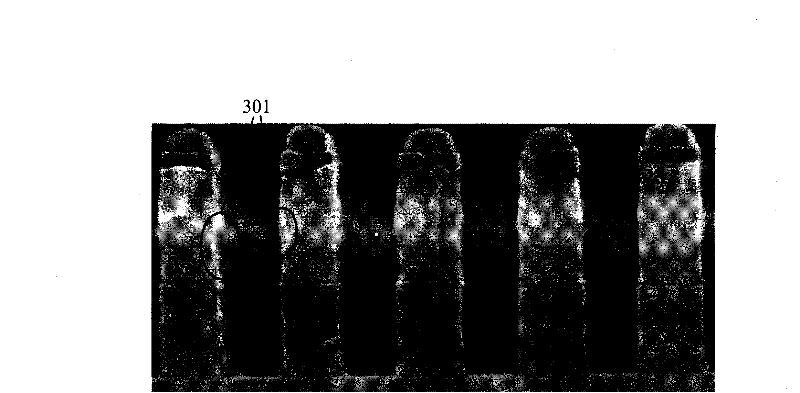
from image 3 From the position 301 circled in the center, it can be seen that a recess will be formed on the side wall of the control gate, thereby reducing the electrical performance of the control gate.

Method used


Image

  • Method for forming flash memory grid electrode and flash memory
  • Method for forming flash memory grid electrode and flash memory
  • Method for forming flash memory grid electrode and flash memory

Examples


Embodiment Construction

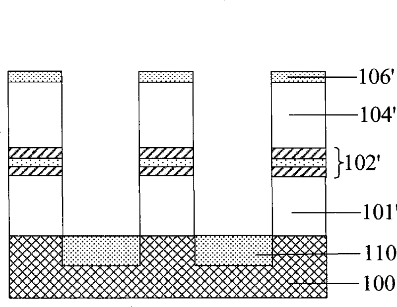
[0023] The inventors found that if figure 2 As shown, since the existing flash memory gate structure is a stacked structure of the floating gate 101' and the control gate 104' sandwiching the inter-gate dielectric layer 102'. The main material for forming the floating gate 101' and the control gate 104' is polysilicon. Therefore, during the process of etching to form the floating gate 101', the sidewalls of the unprotected control gate 104' must be eroded by the plasma as an etchant. Although plasma etching is anisotropic etching, the etching rate in the direction parallel to the substrate 100 is much smaller than that in the direction perpendicular to the substrate 100 . However, as the size of the flash memory device gradually decreases, the aspect ratio of the trenches between the gates gradually increases, and the plasma contacts the sidewalls of the control gate 104' relatively more, so the plasma has more contact with the control gate 104'. The erosion of the sidewall...


PUM


Abstract

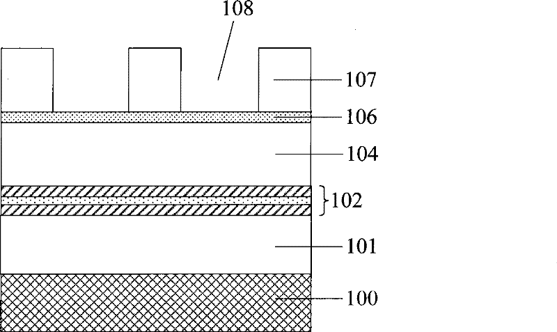
The invention relates to a method for forming a flash memory grid electrode and a flash memory, wherein the method for forming the flash memory grid electrode comprises the following steps of: providing a semiconductor substrate which is covered by a first conducting layer, an inter-grid dielectric layer and a second conducting layer in turn; patterning the second conducting layer until the inter-grid dielectric layer is exposed so as to form a control grid; patterning the inter-grid dielectric layer until the first conducting layer is exposed; after any one of the two steps, forming an atmosphere containing oxygen gas or oxygen plasmas, and forming an oxide film on the side wall of the control grid; and patterning the first conducting layer to form a floating grid. In the method, after the control grid is formed, or after the inter-grid dielectric layer is patterned, the atmosphere containing the oxygen gas or the oxygen plasmas is formed, and the oxide film is formed on the side wall of the control grid, so the side wall of the control grid can be prevented from being damaged in a subsequent step for forming the floating grid, and debosses can be stopped to be formed on the sidewall of the control grid so as to prevent the electrical properties of the control grid from being lowered.

Description

technical field [0001] The present invention relates to the field of fabrication of semiconductor devices, and more particularly, to a method of forming a gate of a flash memory and a flash memory formed thereby. Background technique [0002] At present, flash memory (Flash), also known as flash memory, has become the mainstream of non-volatile memory. According to different structures, flash memory can be divided into two types: NOR Flash and NAND Flash. Among them, or non-flash memory is suitable for applications such as mobile phones or motherboards that need to record system codes because of its fast reading speed. And non-flash memory is especially suitable for multimedia data storage because of its high density and high writing speed. Especially in recent years, NAND flash has been evolving at a rate that keeps doubling its density every year. The latest generation of NAND flash technology has reached a high capacity level of 32Gb per die. In terms of technology, f...

Claims


Application Information

Patent Timeline
Patent Type & Authority Patents(China)
IPC IPC(8): H01L21/28H01L29/788H01L29/423H01L27/115H10B69/00
Inventor 李雪
Owner SEMICON MFG INT (SHANGHAI) CORP
Learn More