Manufacturing method for semi-conductor device with stress memorization function

A manufacturing method and strain memory technology, applied in semiconductor/solid-state device manufacturing, chemical/physical/physicochemical processes of applied energy, electrical components, etc., can solve the problems of electrical performance degradation, limited effect, and overlapping capacitance reduction, etc., to achieve The effect of avoiding the decline of electrical properties

Active Publication Date: 2014-12-24
SEMICONDUCTOR MANUFACTURING INTERNATIONAL (BEIJING) CORP
View PDF2 Cites 0 Cited by
  • Summary
  • Abstract
  • Description
  • Claims
  • Application Information

AI Technical Summary

Problems solved by technology

Wherein, the material of the stress layer 13 is silicon nitride, and hydrogen gas is used as the reaction gas when forming silicon nitride. Therefore, a certain amount of hydrogen atoms are contained in the silicon nitride and the oxide layer 12. Since the silicon nitride material is dense , the hydrogen atoms will not diffuse out of the PMOS tube, the hydrogen atoms will diffuse into the doping region, the doping ions in the doping region disclosed in the paper are boron ions, and the hydrogen atoms will deactivate the boron ions At the same time, the greater pressure of the stress layer 13 on the PMOS tube will cause boron ions to diffuse into the oxide layer 12, thereby causing the overlap capacitance (overlap capacitance) of the PMOS tube to decrease.
[0006] Said paper also published stress layers through porous silicon nitride materials (such as figure 2 The shown stress layer 23) makes the hydrogen atoms diffuse out of the PMOS tube through the pores in the porous silicon nitride, so as to avoid the technical scheme that the overlapping resistance drops, but the effect of the technical scheme is limited
[0007] In the paper "Anomalous Gate Edge Leakage Induced by High Tensile Stress in NMOSFET" published by Po-Tsun Liu et al. (published in IEEE ELECTRONDEVICE LETTERS in 2008), the influence of SMT technology on NMOS tubes was analyzed, in which it was found that , the large tensile stress in the NMOS tube makes the diffusion of the doped region more serious on the one hand, and causes damage to the edge of the gate on the other hand, both of which lead to an increase in the gate channel current
[0008] In summary, for semiconductor devices with strain memory effect (SMT), how to avoid the decline in electrical performance caused by greater stress has become an urgent problem to be solved by those skilled in the art

Method used


Image

  • Manufacturing method for semi-conductor device with stress memorization function
  • Manufacturing method for semi-conductor device with stress memorization function
  • Manufacturing method for semi-conductor device with stress memorization function

Examples


Embodiment Construction

[0035] In order to make the above objects, features and advantages of the present invention more comprehensible, specific implementations of the present invention will be described in detail below in conjunction with the accompanying drawings.

[0036] In the following description, many specific details are set forth in order to fully understand the present invention, but the present invention can also be implemented in other ways than those described here, so the present invention is not limited by the specific embodiments disclosed below.

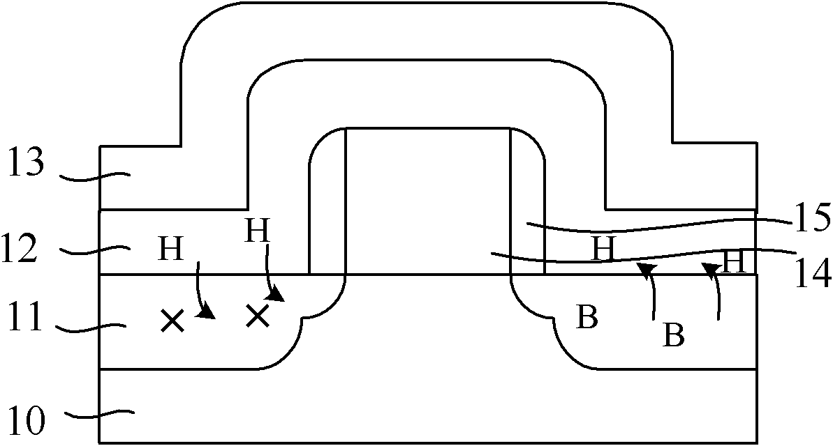
[0037] As described in the background art, in the prior art, the stress provided by the stress layer is relatively large, which will cause performance degradation of the MOS transistor.

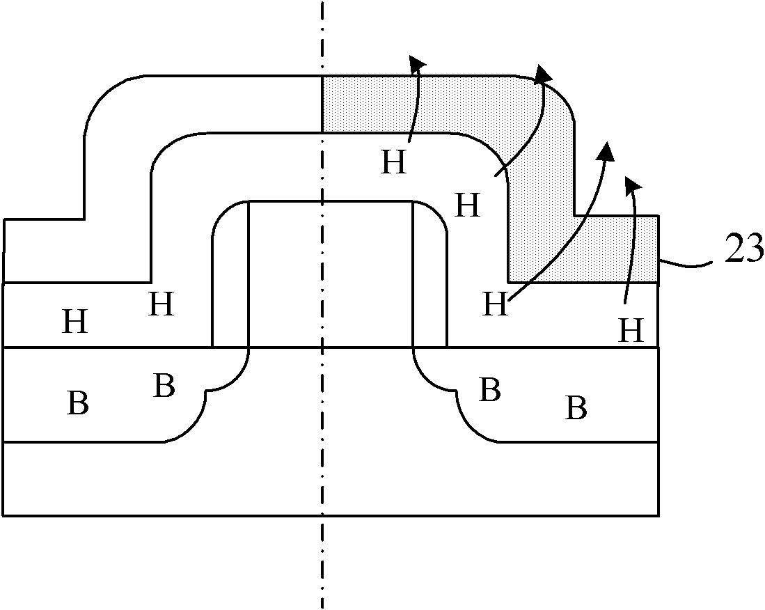
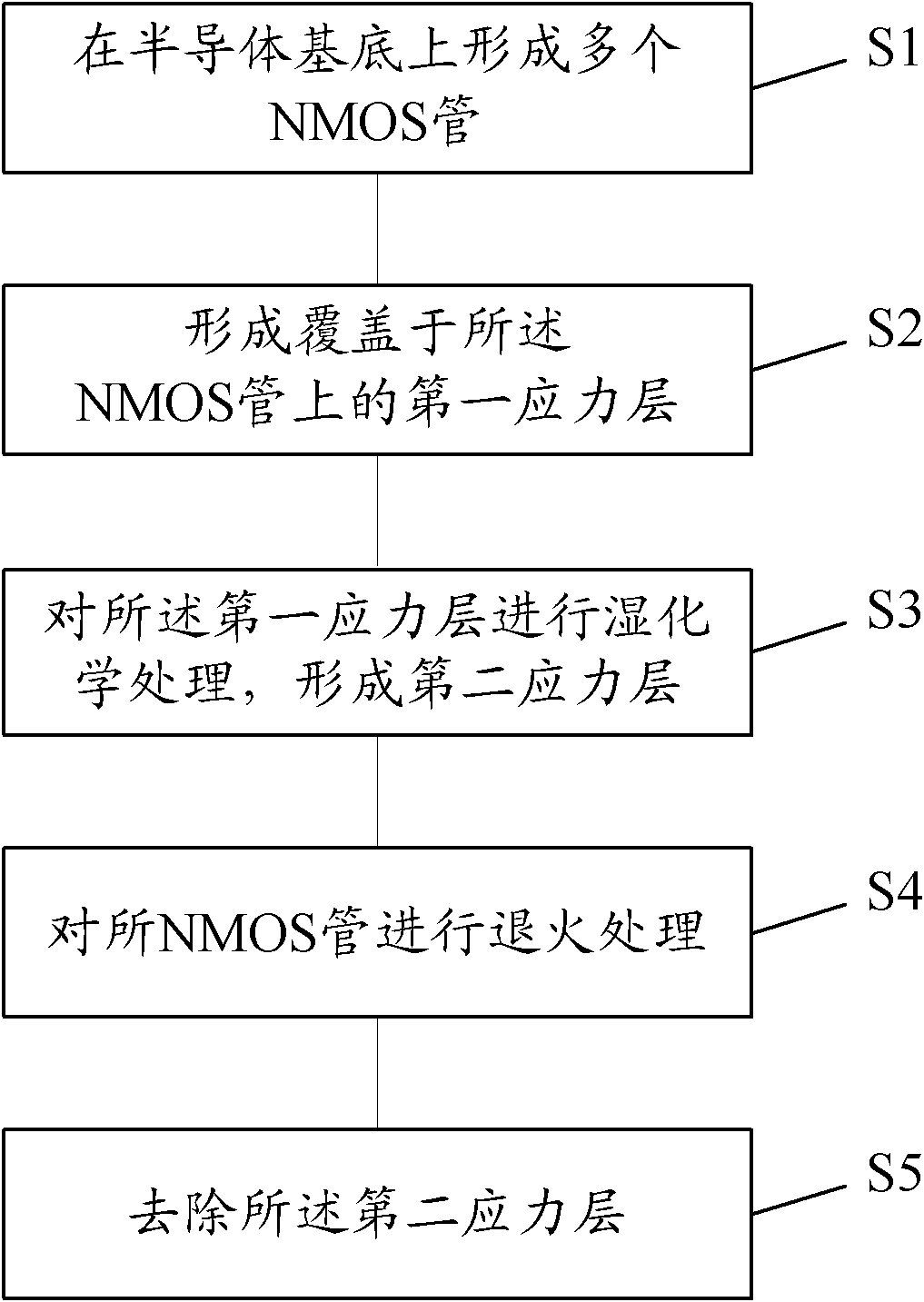
[0038] In view of the above problems, the present invention provides a method for manufacturing a semiconductor device with a strain memory effect. After forming a stress layer on the MOS tube and before performing annealing treatment, the MOS tube is sub...


PUM


Abstract

The invention provides a manufacturing method for a semi-conductor device with a stress memorization function. According to the invention, a plurality of MOS (Metal Oxide Semiconductor) pipes are arranged on a semi-conductor substrate; a first stress layer is arranged on the MOS pipe and comprises a first chemical bond; the first stress layer is subjected to wet-chemical treatment, and a chemical bond combination atom is provided for the first stress layer so as to form a second stress layer including the first chemical bond and a second chemical bond; the stress of the second chemical bond is smaller than that of the first chemical bond; the MOS pipes are subjected to annealing processing; and the second stress layer is removed. The manufacturing method provided by the invention avoids the over stress of the semi-conductor device with the stress memorization function.

Description

technical field [0001] The invention relates to the field of semiconductor manufacturing, in particular to a manufacturing method of a semiconductor device with strain memory function. Background technique [0002] In semiconductor devices, especially MOS devices, one of the main ways to increase the switching frequency of field effect transistors is to increase the driving current, and the main way to increase the driving current is to increase the carrier mobility. An existing technology for improving carrier mobility of field effect transistors is strain memory technology (Stress Memorization Technique, referred to as SMT), which increases carrier mobility in the channel by forming stable stress in the channel region of the field effect transistor. Generally, tensile stress can make the molecular arrangement in the channel region more loose, thereby improving the mobility of electrons, which is suitable for NMOS transistors; while compressive stress can make the molecular...

Claims


Application Information

Patent Timeline
Patent Type & Authority Patents(China)
IPC IPC(8): H01L21/8238H01L21/336B01J19/10
Inventor 三重野文健
Owner SEMICONDUCTOR MANUFACTURING INTERNATIONAL (BEIJING) CORP
Why Eureka
Try Eureka