
Multilayer LED chip structure and preparation method thereof

A technology of LED chips and buffer layers, applied in electrical components, circuits, semiconductor devices, etc., can solve problems such as the inability to meet the requirements of high-power, high-efficiency LEDs and LDs

Inactive Publication Date: 2010-06-09
INST OF SEMICONDUCTORS - CHINESE ACAD OF SCI
View PDF0 Cites 19 Cited by
  • Summary
  • Abstract
  • Description
  • Claims
  • Application Information

AI Technical Summary

Problems solved by technology

[0006] Although the quality of the GaN epitaxial film prepared by this method has been greatly improved, it still cannot meet the current requirements for high-power, high-efficiency LEDs and LDs.
First of all, the epitaxial GaN material on the sapphire substrate has a large number of dislocations in the LED structure due to the large lattice mismatch and the difference in thermal expansion coefficient.
Secondly, in the epitaxial LED structure on the sapphire (0001) surface, in the quantum well area where the light is emitted, the quantum confinement Stark effect caused by the piezoelectric polarization and spontaneous polarization effects

Method used


Image

  • Multilayer LED chip structure and preparation method thereof
  • Multilayer LED chip structure and preparation method thereof
  • Multilayer LED chip structure and preparation method thereof

Examples


Embodiment Construction

[0048] In order to make the objectives, technical solutions, and advantages of the present invention clearer, the following further describes the present invention in detail in conjunction with specific embodiments and with reference to the accompanying drawings.

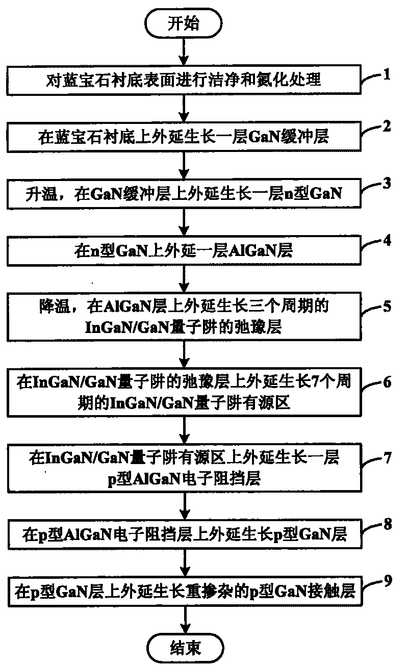
[0049] Such as figure 1 As shown, figure 1 It is a flow chart of a method for preparing a multilayer LED chip structure provided by the present invention. The method includes the following steps:

[0050] Step 1: Cleaning and nitriding the surface of the sapphire substrate;

[0051] In this step, cleaning and nitriding the surface of the sapphire substrate specifically includes: putting the sapphire substrate at a high temperature of 1100°C and using H 2 The surface of the substrate is cleaned; then the temperature is reduced to 500° C., and the surface of the sapphire substrate is nitridated.

[0052] Step 2: epitaxially grow a GaN buffer layer on the processed sapphire substrate;

[0053] In this step, a GaN buffer layer wi...


PUM

PropertyMeasurementUnit
Growth temperatureaaaaaaaaaa
Thicknessaaaaaaaaaa

Abstract

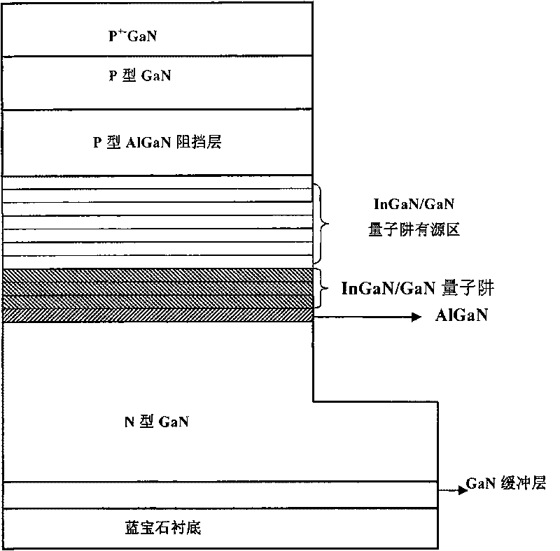
The invention discloses a multilayer LED chip structure and a preparation method thereof. The structure comprises a sapphire substrate, a GaN buffer layer formed on the sapphire substrate through low temperature epitaxial growth, a n-type GaN formed on the GaN buffer layer through high temperature epitaxial growth, an AlGaN layer formed on the n-type GaN through high temperature epitaxial growth, an InGaN / GaN quantum well relaxation layer growing on the AlGaN layer for three periods, an InGaN / GaN quantum well active area growing on the InGaN / GaN quantum well relaxation layer for seven periods, a p-type AlGaN electronic blocking layer growing on the InGaN / GaN quantum well active area, a p-type GaN layer growing on the electronic blocking layer and a heavily-doped p-type GaN contact layer growing on the p-type GaN layer. The structure can effectively reduce the dislocation density of a material in an epitaxial layer, reduces the influence of quantum-confined Stark effect, and improves the internal quantum efficiency of an LED.

Description

Technical field [0001] The invention relates to the technical field of solid-state lighting, in particular to a multilayer LED chip structure grown by MOCVD and a preparation method thereof. The epitaxial LED chip under this structure can effectively improve the internal quantum luminous efficiency and light extraction efficiency inside the material. Background technique [0002] The world consumes a lot of energy every year, of which lighting electricity accounts for about 20% of the total electricity consumption. Fluorescent lamps and incandescent lamps are now widely used lighting sources, but they have a big defect, that is, the luminous efficiency is too low, and 40% of the lighting power is consumed by them. The incandescent lamp emits white light by means of thermal radiation. Although its color rendering effect is very good, its efficiency is very low. Only 10% of the electric energy can emit light. Fluorescent lights are slightly better, but not very efficient. The ty...

Claims


Application Information

Patent Timeline
IPC IPC(8): H01L33/06
Inventor 李京波朱峰纪攀峰
Owner INST OF SEMICONDUCTORS - CHINESE ACAD OF SCI
Learn More